Rapid fault tolerance method of normally open faults of nanometer CMOS circuit
A defect and nano technology, applied in the field of nano-CMOS circuit fault-tolerant mapping, can solve the problems of low mapping success rate, poor solution quality, slow mapping method speed, etc., and achieve the effect of reducing the mapping area, eliminating the influence and simplifying the difficulty.
- Summary
- Abstract
- Description
- Claims
- Application Information
AI Technical Summary
Problems solved by technology
Method used
Image
Examples
Embodiment 1
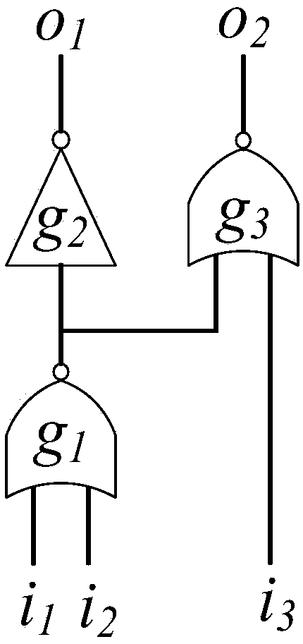
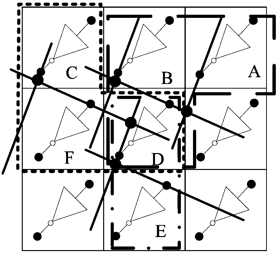
[0042] Embodiment 1: Take the simple circuit of three inputs and two outputs shown in Fig. 2 (a) as an example to carry out layering, and its fault-tolerant mapping layered schematic diagram on the defective nanometer CMOS circuit is shown in Figure 4 , 3 input terminals and 3 nodes are respectively mapped on the unit A-E unit, in which the nanodiode 1 between unit BD has a normally-on defect, the output nanowire of unit C is broken at 2, and the bottom CMOS unit of unit E is at 3 There is an unavailable normally open defect. Figure 4 The fast fault-tolerant method for the shown nanometer CMOS circuit includes the following steps:
[0043] Step ①: According to formula (1), calculate the total number of effective defects in the nano-CMOS circuit n def =5; Calculate y (0)=2, y (1)=2, y (2)=1 according to the defect distribution function of formula (2); From the boundary first unit of nanometer CMOS circuit, check unit C, successively B. The CMOS stack defects of A. After ins...
Embodiment 2
[0051] Embodiment 2: with Figure 5 The nano-CMOS circuit structure with a size of 5×4 is shown as an example, and the schematic diagram of the normally-on defect of the nano-diode is shown in Figure 5 .
[0052] Figure 5 The nano-CMOS circuit structure shown includes 20 nano-CMOS units, and the input nanowire of unit F can receive the output signals of unit A and unit B through programmable nano-diodes, and the The logic function; the input nanowire of unit F' can receive the output signal of unit C and unit D, and complete the logic function from Figure 5 It can be seen that the programmable nanodiode located at the intersection of the output nanowire of B and the input nanowire of F is normally on ( Figure 5 Indicated by the square 1 in the center), the programmable nanodiode located at the intersection of the output nanowire of D and the input nanowire of F' is normally open ( Figure 5 Indicated by square 2 in the middle), the actual logical function that can b...
Embodiment 3
[0058] Embodiment 3: with Image 6 The nano-CMOS circuit structure of 8×8 size is shown as an example, and the schematic diagram of its nano-diode normally-on defect is shown in Image 6 .
[0059] When the output nanowire of unit A breaks at point a, the nanodiodes connected to the nanowire at point a and the nanometer CMOS circuit units connected to these nanodiodes cannot receive the output signal of unit A. For unit A, the range of the output connected domain of A is narrowed, and the basic function of the nano-CMOS circuit unit connected below point a remains unchanged, but the total number of units in the input connected domain is reduced by one unit A. Therefore, as long as the associated nodes avoid mapping nano-CMOS cells with broken nanowires and connected nano-CMOS cells beyond the broken point, the defective cells can continue to be used.
[0060] Image 6 The fast fault-tolerant method for the normally-on defect of the shown nanometer CMOS circuit comprises the...
PUM
 Abstract
Description
Claims
Application Information
 - R&D Engineer
- R&D Manager
- IP Professional
- Industry Leading Data Capabilities
- Powerful AI technology
- Patent DNA Extraction
Browse by: Latest US Patents, China's latest patents, Technical Efficacy Thesaurus, Application Domain, Technology Topic, Popular Technical Reports.
© 2024 PatSnap. All rights reserved.Legal|Privacy policy|Modern Slavery Act Transparency Statement|Sitemap|About US| Contact US: help@patsnap.com


