Quantum dot electroluminescent device and display
An electroluminescent device and quantum dot technology, applied in the field of quantum dots, can solve the problems of different transmission rates between electrons and holes, positive load carrier imbalance, etc., and achieve the goals of reducing space charge accumulation, good current efficiency, and improving efficiency Effect
- Summary
- Abstract
- Description
- Claims
- Application Information
AI Technical Summary
Problems solved by technology
Method used
Image
Examples
Embodiment 1
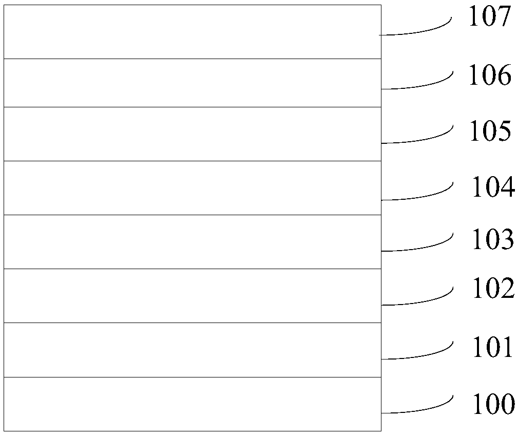
[0051] This embodiment provides a quantum dot electroluminescent device with a structure such as figure 1 As shown, the substrate 100, the first electrode layer 101, the hole injection layer 102, the hole transport layer 103, the light emitting layer 104, the first electron transport layer 105, the second electron transport layer 106 and the second electrode layer 107;
[0052] The material of the first electron transport layer 105 is ZnO; the material of the second electron transport layer 106 is TmPyPB:LiQ.
[0053] The preparation process of the quantum dot electroluminescent device of the present embodiment is as follows:
[0054] (1) The glass substrate containing the ITO (120nm) transparent electrode was cleaned with deionized water and isopropanol and continuously ultrasonicated for 25 minutes, then dried with a nitrogen gun, and treated under UV-O for 20 minutes to clean The surface of ITO, and improve the work function of ITO;
[0055] (2) Deposit a hole injection ...
Embodiment 2
[0062] This embodiment provides a quantum dot electroluminescent device, in which a substrate 100, a first electrode layer 101, a hole injection layer 102, a hole transport layer 103, a light emitting layer 104, and a first electron transport layer 105 are sequentially stacked from bottom to top , the second electron transport layer 106 and the second electrode layer 107;
[0063] The material of the first electron transport layer 105 is MgO; the material of the second electron transport layer 106 is TmPyPB:LiQ.
[0064] The preparation process of the quantum dot electroluminescent device of the present embodiment is as follows:
[0065] (1) The glass substrate containing the ITO (120nm) transparent electrode was cleaned with deionized water and isopropanol and continuously ultrasonicated for 25 minutes, then dried with a nitrogen gun, and treated under UV-O for 20 minutes to clean The surface of ITO, and improve the work function of ITO;
[0066] (2) Deposit a hole injectio...
Embodiment 3
[0073] This embodiment provides a quantum dot electroluminescent device, in which a substrate 100, a first electrode layer 101, a hole injection layer 102, a hole transport layer 103, a light emitting layer 104, and a first electron transport layer 105 are sequentially stacked from bottom to top , the second electron transport layer 106 and the second electrode layer 107;
[0074] The material of the first electron transport layer 105 is TiO 2 ; The material of the second electron transport layer 106 is Bphen:LiQ.
[0075] The preparation process of the quantum dot electroluminescent device of the present embodiment is as follows:
[0076] (1) The glass substrate containing the ITO (120nm) transparent electrode was cleaned with deionized water and isopropanol and continuously ultrasonicated for 25 minutes, then dried with a nitrogen gun, and treated under UV-O for 20 minutes to clean The surface of ITO, and improve the work function of ITO;
[0077] (2) Deposit a hole injec...
PUM
 Abstract
Description
Claims
Application Information
 - R&D
- Intellectual Property
- Life Sciences
- Materials
- Tech Scout
- Unparalleled Data Quality
- Higher Quality Content
- 60% Fewer Hallucinations
Browse by: Latest US Patents, China's latest patents, Technical Efficacy Thesaurus, Application Domain, Technology Topic, Popular Technical Reports.
© 2025 PatSnap. All rights reserved.Legal|Privacy policy|Modern Slavery Act Transparency Statement|Sitemap|About US| Contact US: help@patsnap.com


