A graphene field effect transistor array biosensor and its preparation method and detection method
A field-effect transistor, array biology technology, applied in instruments, measuring devices, scientific instruments, etc., can solve problems such as low accuracy and separation of objects to be measured.
- Summary
- Abstract
- Description
- Claims
- Application Information
AI Technical Summary
Problems solved by technology
Method used
Image
Examples
specific Embodiment approach 1
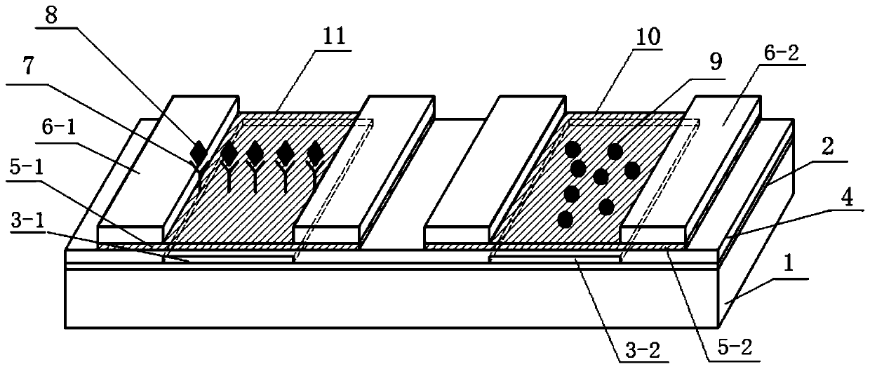
[0043] Specific implementation mode one: the following combination figure 1 This embodiment will be specifically described. The graphene field effect transistor array biosensor of the present embodiment consists of a silicon substrate 1, an oxide layer 2, a first metal gate 3-1, a second metal gate 3-2, a gate insulating layer 4, a first graphene conductive The channel layer 5-1, the second graphene conductive channel layer 5-2, the first group of source and drain electrodes 6-1 and the second group of source and drain electrodes 6-2 are composed of:
[0044] An oxide layer 2 is provided on the silicon substrate 1, a first metal gate 3-1 and a second metal gate 3-2 are symmetrically provided on the oxide layer 2, and the first metal gate 3-1 and the second metal gate 3-2 is provided with a gate insulating layer 4 outside, and the gate insulating layer 4 completely covers the first metal gate 3-1 and the second metal gate 3-2, and the gate insulating layer 4 is symmetrically p...
specific Embodiment approach 2
[0049] Specific embodiment 2: The difference between this embodiment and specific embodiment 1 is that the material of the first metal grid 3-1 and the second metal grid 3-2 is Ti / Pt, wherein the thickness of Ti is 100nm ~110nm, the thickness of Pt is 200nm~210nm. Others are the same as in the first embodiment.
specific Embodiment approach 3
[0050] Specific embodiment three: the preparation method of a kind of graphene field effect transistor array biosensor of present embodiment is carried out according to the following steps:
[0051] 1. Production of transistor structure:
[0052] a. Silicon substrate cleaning:
[0053] Cleaning the silicon wafer to obtain a silicon substrate 1;
[0054] b. Thermal oxidation growth of SiO 2 As an insulating layer:
[0055] The silicon substrate 1 is sequentially subjected to dry oxygen oxidation, wet oxygen oxidation and dry oxygen oxidation, specifically according to the following steps: under the conditions of a temperature of 1050° C. to 1055° C. and an air velocity of 24 cm / s to 26 cm / s, Dry oxygen oxidation for 4 minutes to 6 minutes, then wet oxygen oxidation for 5 minutes to 7 minutes at a temperature of 1050°C to 1055°C and an air velocity of 0.8 cm / s to 1.2 cm / s, and finally at a temperature of 1050°C to 1055°C and Under the condition of air velocity of 24 cm / s-26 ...
PUM
| Property | Measurement | Unit |
|---|---|---|
| thickness | aaaaa | aaaaa |
| thickness | aaaaa | aaaaa |
| thickness | aaaaa | aaaaa |
Abstract
Description
Claims
Application Information
 - R&D
- Intellectual Property
- Life Sciences
- Materials
- Tech Scout
- Unparalleled Data Quality
- Higher Quality Content
- 60% Fewer Hallucinations
Browse by: Latest US Patents, China's latest patents, Technical Efficacy Thesaurus, Application Domain, Technology Topic, Popular Technical Reports.
© 2025 PatSnap. All rights reserved.Legal|Privacy policy|Modern Slavery Act Transparency Statement|Sitemap|About US| Contact US: help@patsnap.com


