Eureka AIR delivers breakthrough ideas for toughest innovation challenges, trusted by R&D personnel around the world.

Method for preventing solder mask ink from plugging hole, printed circuit board and computer device

A printed circuit board, solder mask ink technology, applied in the directions of printed circuit, printed circuit manufacturing, printed circuit secondary processing, etc., can solve the problem of not completely eliminating the phenomenon of plugging holes, non-plugging ink blocking holes, and high blocking ratio. , to achieve the effect of preventing non-plugging ink from blocking holes, reducing scrap, and avoiding alignment accuracy.

Inactive Publication Date: 2018-12-04
PEKING UNIV FOUNDER GRP CO LTD +1
View PDF3 Cites 8 Cited by
  • Summary
  • Abstract
  • Description
  • Claims
  • Application Information

AI Technical Summary

Problems solved by technology

[0002] With the increasing application of printed circuit boards, the requirements for corresponding circuit boards have also changed. In the case of through-hole solder masking, there are requirements for making plugged holes, non-plugged holes, oil-covered holes, and window openings at the same time. Due to the limitation of the production process, the phenomenon of non-plugging ink blocking the hole occurs. The traditional production method is to use the dot screen printing oil, but this method cannot be completely eliminated due to the limitation of the expansion and contraction of the printed circuit board and the dot network and the alignment accuracy. Hole blocking phenomenon, especially for plates with small holes and high thickness-to-diameter ratio.

Method used


Image

  • Method for preventing solder mask ink from plugging hole, printed circuit board and computer device
  • Method for preventing solder mask ink from plugging hole, printed circuit board and computer device
  • Method for preventing solder mask ink from plugging hole, printed circuit board and computer device

Examples


Embodiment Construction

[0039] In order to understand the above-mentioned purpose, features and advantages of the present invention more clearly, the present invention will be further described in detail below in conjunction with the accompanying drawings and specific embodiments. It should be noted that, in the case of no conflict, the embodiments of the present application and the features in the embodiments can be combined with each other.

[0040] In the following description, many specific details are set forth in order to fully understand the present invention, but the present invention can also be implemented in other ways different from those described here, therefore, the protection scope of the present invention is not limited to the specific details disclosed below. EXAMPLE LIMITATIONS.

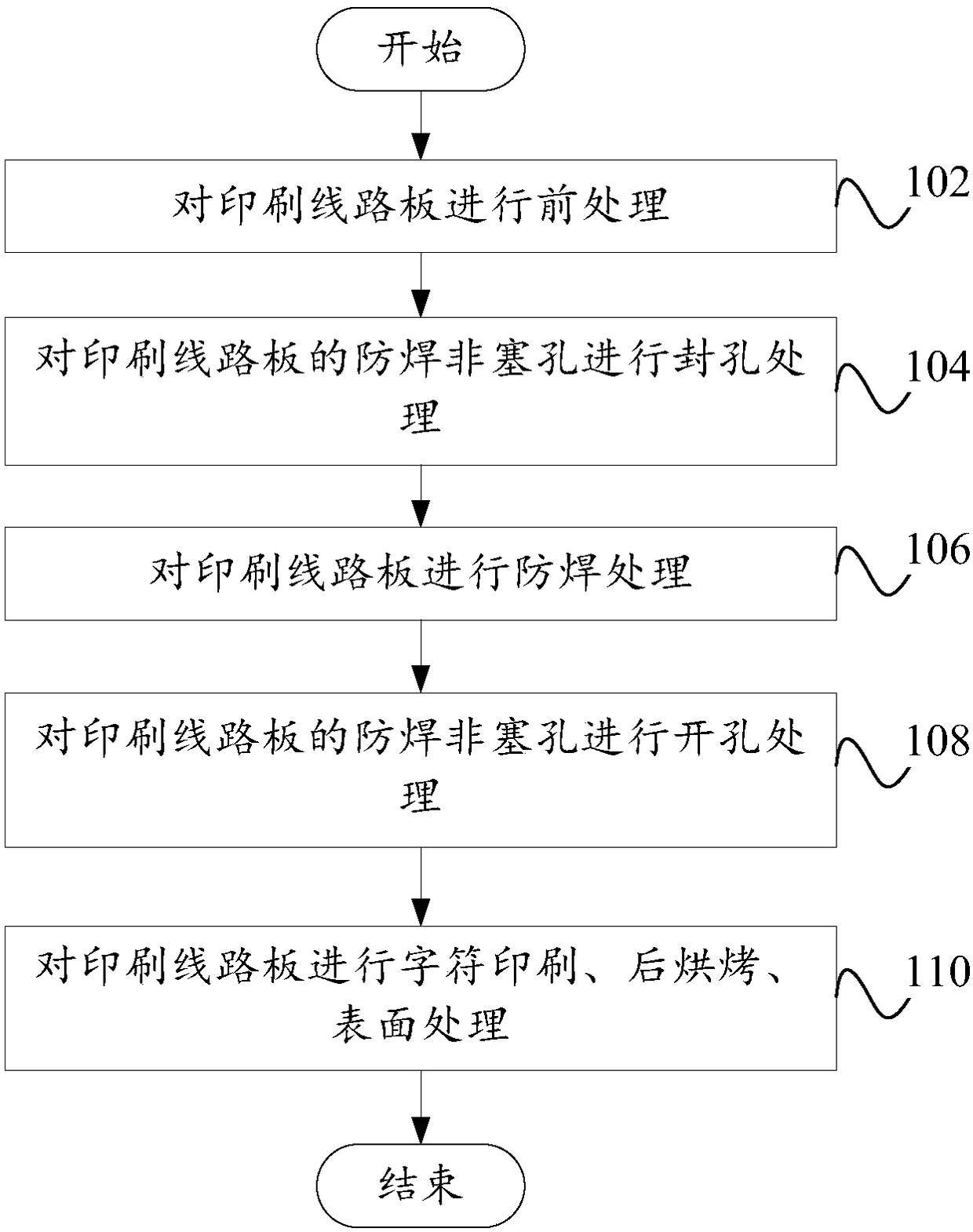
[0041] In the embodiment of the first aspect of the present invention, a method for preventing hole blocking by solder resist ink is proposed, Figure 1a A schematic flow chart of a method for preventing ...


PUM


Abstract

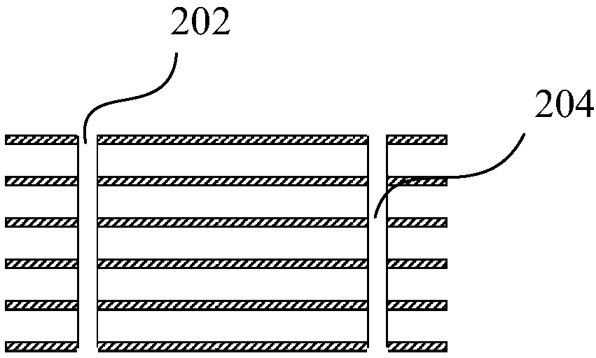
The invention provides a method for preventing solder mask ink from plugging a hole, a printed circuit board, a computer device and a computer readable storage medium. The method for preventing the solder mask ink from plugging the hole comprises the following steps: a solder mask non-plugging hole of the printed circuit board is subjected to hole sealing operation; solder masking operation is performed on the printed circuit board; the solder mask non-plugging hole of the printed circuit board is subjected to hole opening operation. The method disclosed in the present invention can help prevent the non-plugging hole from being plugged by ink, the method can help prevent a problem of printed circuit board and blocking point net expansion and shrinkage that occurs when block point net ink is used and a problem of alignment precision, scrapping of the printed circuit board which is caused when the hole is plugged by ink can be reduced, and high reliability and high efficiency can be realized.

Description

technical field [0001] The invention relates to the technical field of printed circuit boards, in particular to a method for preventing holes blocked by solder resist ink, a printed circuit board, a computer device and a computer-readable storage medium. Background technique [0002] With the increasing application of printed circuit boards, the requirements for corresponding circuit boards have also changed. In the case of through-hole solder masking, there are requirements for making plugged holes, non-plugged holes, oil-covered holes, and window openings at the same time. Due to the limitation of the production process, the phenomenon of non-plugging ink blocking the hole occurs. The traditional production method is to use the dot screen printing oil, but this method cannot be completely eliminated due to the limitation of the expansion and contraction of the printed circuit board and the dot network and the alignment accuracy. Hole blocking phenomenon, especially for pla...

Claims


Application Information

Patent Timeline
Patent Type & Authority Applications(China)
IPC IPC(8): H05K3/28
CPCH05K3/282H05K2203/1438
Inventor 吴世平胡新星李晓胡永栓
Owner PEKING UNIV FOUNDER GRP CO LTD
Why Eureka
Eureka Blog
Learn More