


Quick Research
Generate reliable direction feasibility study reports for your R&D in just a few steps.

Technical Q&A
Discover and master advanced knowledge NOW. Basics, ideas, possibilities, all at once.

Find Solutions
As an expert in R&D theories, this can generate solutions to your technical problems instantly.

Evaluate Feasibility
Analyze your overall solution with one click, know your potential R&D risks in advance.

Monitor Landscape
Get weekly tech updates, stay abreast of the latest tech innovations and key insights.
Test system, method and device
A test system and test signal technology, applied in the direction of measurement device, measurement of electricity, measurement of electric variables, etc., can solve the problems of long calibration time, complex test system, low test efficiency, etc., to achieve low test cost, reduce test process, The effect of improving test efficiency
- Summary
- Abstract
- Description
- Claims
- Application Information
AI Technical Summary
Problems solved by technology
Method used
Image

Examples
Embodiment 1
[0034] Optionally, the programmable gate array (such as XC7Z030) in the present invention may also include an embedded ARM processor, which can realize software control of the entire pre-test system.
[0035] Therefore, in the present invention, the programmable gate array is used to generate the test signal and the interference signal at the same time, so as to realize the performance detection of the device to be tested. After the device under test receives the signal, if it is judged that the signal is consistent with the preset test signal, it means that the device under test receives the signal successfully. If not, it means that the device under test fails to receive the signal this time.
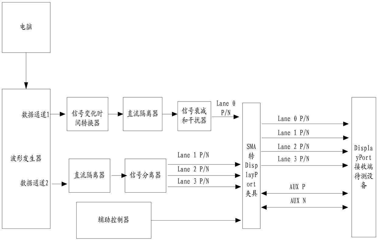
[0036] For the actual physical layer test of the receiving end of the device under test, it can be divided into pre-test and formal test. The pre-test is responsible for confirming whether the device under test supports the basic process of physical layer testing, as well as the recep...
Embodiment 2
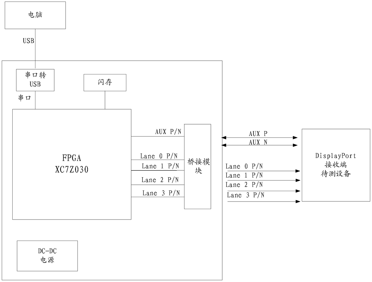
[0051] image 3 is a schematic diagram of another optional test system according to an embodiment of the present invention, such as image 3 As shown, the test system includes: computer (corresponding to the above-mentioned external machine terminal equipment), FPGA XC7Z030 (corresponding to the above-mentioned programmable gate array FPGA), flash memory (can be falsh flash memory), serial port to USB, bridge module (as Signal transmission module), DC-DC power supply, DisplayPort receiving end equipment under test.
[0052] In the embodiment of the present invention, a Xilinx FPGA XC7Z030 is used as a main link generator and an auxiliary controller. XC7Z030 can have four sets of independent high-speed serial transceivers GTX, and each set can support a maximum transmission rate of 12.5Gbps. Currently, the maximum transmission rate of the DisplayPort standard is 8.1Gbps. XC7Z030 can fully support all current DisplayPort transmission rates. In terms of quantity, it can also ...
Embodiment 3
[0064] According to an embodiment of the present invention, an embodiment of a testing method is provided. It should be noted that the steps shown in the flow charts of the accompanying drawings can be executed in a computer system such as a set of computer-executable instructions, and, although in The flowcharts show a logical order, but in some cases the steps shown or described may be performed in an order different from that shown or described herein.
[0065] Figure 5 It is a flowchart of a test method according to an embodiment of the present invention, which is applied to any of the above test systems, such as Figure 5 As shown, the method includes the following steps:
[0066] Step S102, detecting whether a test instruction triggered by a test operation is received.
[0067] Step S104, after receiving the test instruction, determine the target link rate and the target channel.
[0068] Step S106, according to the target link rate and the target channel, send a tes...
PUM
 Abstract
Description
Claims
Application Information
 - R&D Engineer
- R&D Manager
- IP Professional
- Industry Leading Data Capabilities
- Powerful AI technology
- Patent DNA Extraction
Browse by: Latest US Patents, China's latest patents, Technical Efficacy Thesaurus, Application Domain, Technology Topic, Popular Technical Reports.
© 2024 PatSnap. All rights reserved.Legal|Privacy policy|Modern Slavery Act Transparency Statement|Sitemap|About US| Contact US: help@patsnap.com