A common voltage generating circuit, a source driving circuit and a liquid crystal display device
A common voltage and circuit generation technology, applied in static indicators, instruments, etc., can solve the problem of liquid crystal display panel inversion and other problems, and achieve the effect of avoiding the phenomenon of inversion.
- Summary
- Abstract
- Description
- Claims
- Application Information
AI Technical Summary
Problems solved by technology
Method used
Image
Examples
no. 1 example
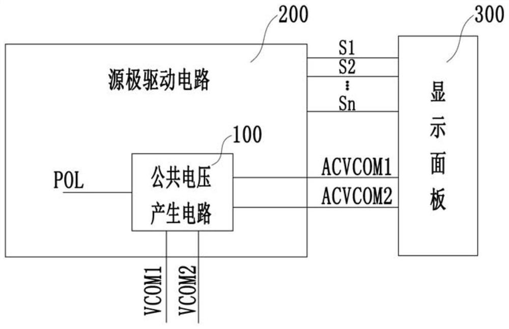
[0025]Please refer tofigure 1 ,figure 1 It is a schematic diagram of the connection of the common voltage generating circuit of an embodiment. Such asfigure 1 As shown, the common voltage generating circuit of this embodiment includes a common voltage generating circuit 100. The common voltage generating circuit 100 receives a first common voltage VCOM1 and a second common voltage VCOM2, and reverses the polarity according to the output of the source driving circuit 200 The control signal POL outputs the first AC common voltage ACVCOM1 and the second AC common voltage ACVCOM2 with opposite polarities, and the first AC common voltage ACVCOM1 or the second AC common voltage ACVCOM2 and the source drive circuit 200 output on the corresponding data line Data signal (figure 1 S1, S2...Sn) have the same polarity, and the data signal and the AC common voltage with the same polarity as the data signal act together on the same pixel unit of the display panel 300.
[0026]Specifically, the commo...
no. 2 example
[0032]figure 2 It is a circuit connection diagram of the common voltage generating circuit of an embodiment. Such asfigure 2 As shown, this embodiment provides a specific circuit connection of the common voltage generating circuit 100 in the common voltage generating circuit. The common voltage generating circuit 100 includes a first switching element T1, a second switching element T2, a third switching element T3, a fourth switching element T4, and a first inverting element 101. The first switching element T1 includes a first control terminal, a first path terminal, and a second path terminal. The first control terminal of the first switching element T1 receives the polarity inversion control signal POL, and the second path terminal of the first switching element T1 Receive the second common voltage VCOM2. The second switching element T2 includes a second control terminal, a third channel terminal, and a fourth channel terminal. The second control terminal of the second switching e...
no. 3 example
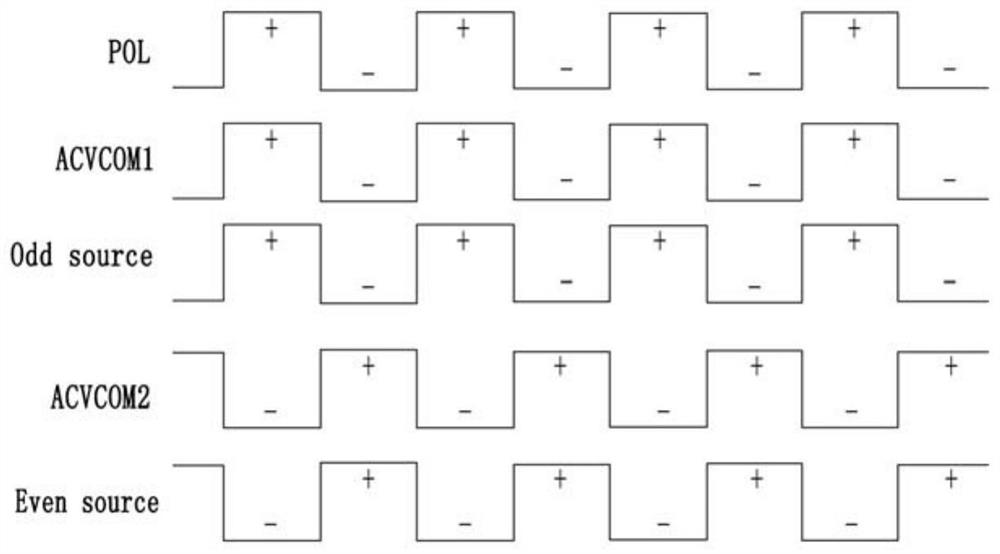
[0042]image 3 It is a related waveform diagram of the output voltage of the common voltage generating circuit of an embodiment. In this example, the first AC common voltage ACVCOM1 and the source drive circuit 200 have the same polarity of the data signal output on the odd column data line, and the second AC common voltage ACVCOM2 and the source drive circuit 200 are on the even column data line. The polarity of the data signal output on theimage 3 Waveform diagram shown.
[0043]Specifically, the first AC common voltage ACVCOM1 and the second AC common voltage ACVCOM2 are inverted with each polarity inversion of the polarity inversion control signal POL, and the first AC common voltage ACVCOM1 and the source The polarity of the data signal Odd Source output by the pole drive circuit 200 on the data line of the odd column is consistent, so that the first AC common voltage ACVCOM1 and the data signal Odd Source output by the source drive circuit 200 on the data line of the odd column wo...
PUM
 Abstract
Description
Claims
Application Information
 - R&D
- Intellectual Property
- Life Sciences
- Materials
- Tech Scout
- Unparalleled Data Quality
- Higher Quality Content
- 60% Fewer Hallucinations
Browse by: Latest US Patents, China's latest patents, Technical Efficacy Thesaurus, Application Domain, Technology Topic, Popular Technical Reports.
© 2025 PatSnap. All rights reserved.Legal|Privacy policy|Modern Slavery Act Transparency Statement|Sitemap|About US| Contact US: help@patsnap.com


