
Packaging method of three-dimensional heterostructure for realizing heat dissipation of high power GaN device layer

A technology of heterogeneous structure and packaging method, which is applied in the fields of electrical solid-state devices, semiconductor devices, semiconductor/solid-state device manufacturing, etc. Power GaN chip three-dimensional integrated packaging heat flux and other issues, to achieve high manufacturability, efficient heat dissipation efficiency, and high stability

Active Publication Date: 2018-11-06
XIAMEN UNIV
View PDF8 Cites 40 Cited by
  • Summary
  • Abstract
  • Description
  • Claims
  • Application Information

AI Technical Summary

Problems solved by technology

Generally speaking, heat sink heat dissipation technology uses composite metal materials with low thermal diffusivity to make miniature heat sinks to achieve cooling of electronic chip devices. The demand for miniaturization is an effective way to reduce chip temperature and ensure device performance, but the external heat sink cooling structure is not conducive to high-density, miniaturized 3D integrated packaging, and the heat dissipation capacity is also insufficient to meet the requirements of high-power GaN chip 3D integrated packaging. heat flux

Method used


Image

  • Packaging method of three-dimensional heterostructure for realizing heat dissipation of high power GaN device layer
  • Packaging method of three-dimensional heterostructure for realizing heat dissipation of high power GaN device layer
  • Packaging method of three-dimensional heterostructure for realizing heat dissipation of high power GaN device layer

Examples


Embodiment 1

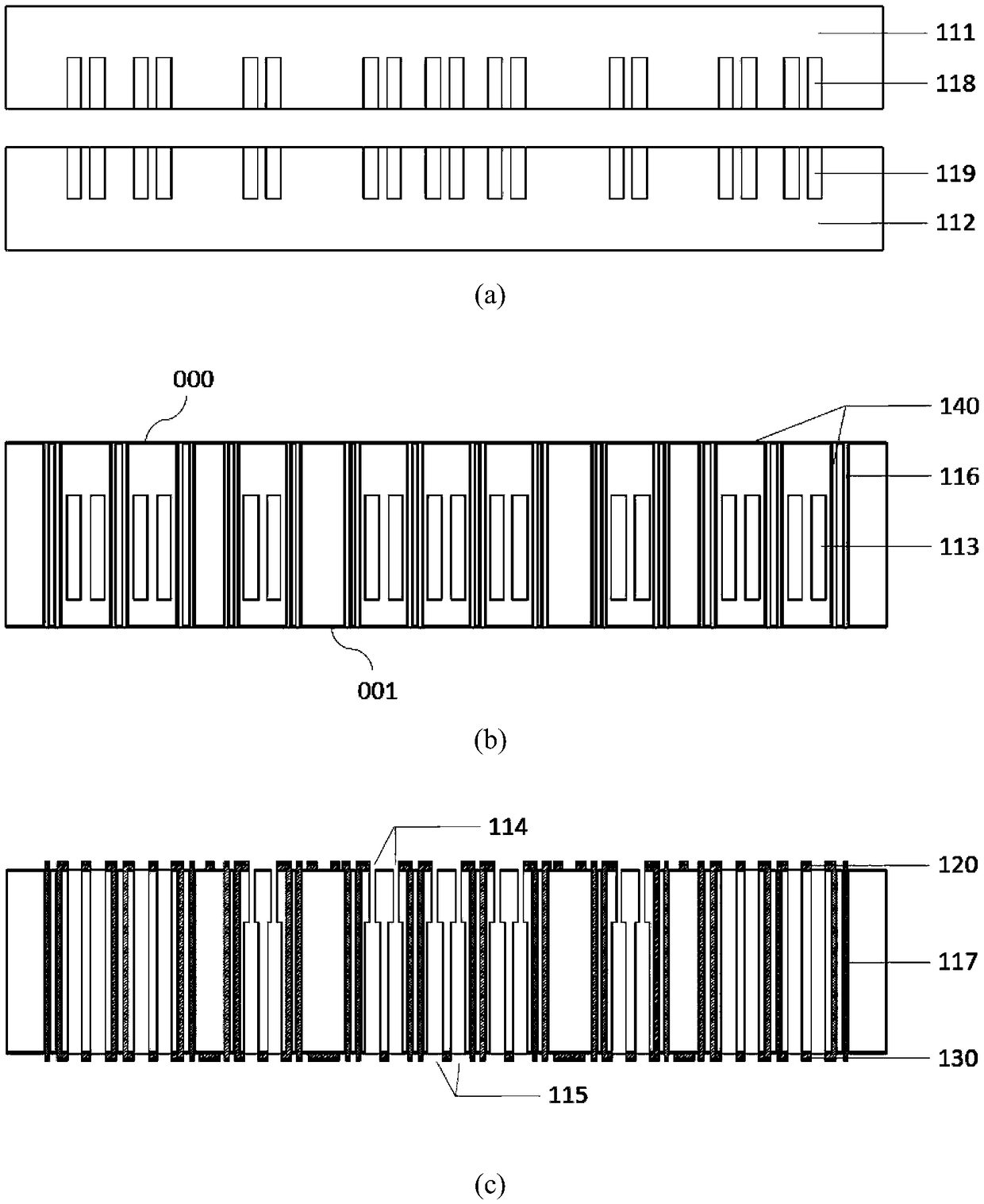
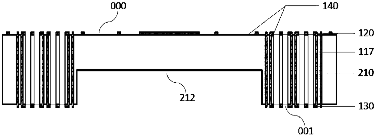
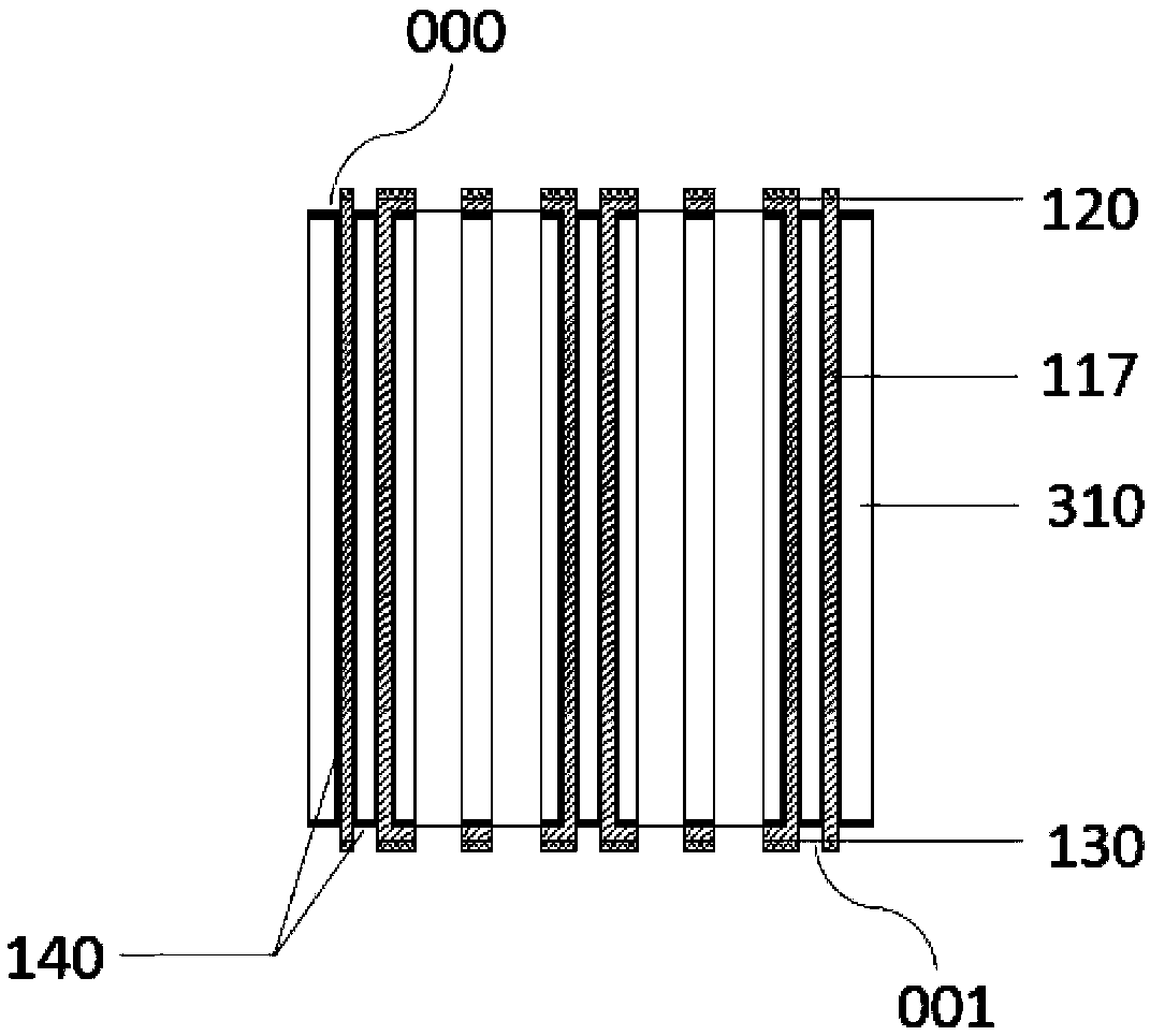
[0044] A packaging structure of a three-dimensional heterogeneous structure that realizes heat dissipation of high-power GaN device layers, such as Figure 4-6 shown, including:

[0045] The first substrate 110, the first substrate 110 made of a high-resistance silicon material (≥1000Ω·cm) substrate is composed of a first substrate 111 and a second substrate 112, and the first substrate 110 has a front surface 000 and A back surface 001, the first substrate 110 includes a certain depth of first vertical micro-channels 113 and vertical interconnection structures. The front 000 of the first substrate 110 is provided with a microchannel output port 114 corresponding to the size of the embedded microchannel structure, and the back 001 is provided with a microchannel input port 115 corresponding to the size of the embedded microchannel structure 113; The vertical interconnection structure is formed by the following structure: the first substrate 110 is provided with a plurality of...


PUM


Abstract

The invention proposes a packaging method of a three-dimensional heterostructure for realizing heat dissipation of a high power GaN device layer for the integrated requirements of three-dimensional heterostructure integration of a high power GaN device and the heat dissipation of a device layer. A three-dimensional folding micro-channel design is realized by utilizing a plurality of laminated substrates such as a GaN chip body-TSV radio frequency adapter plate-silicon supporting block; a microfluid flows in from the bottom layer of a packaging shell and then steps up to cool a GaN device layer hot spot and then steps down and flows out, therefore, the problems in a traditional TSV three-dimensional integration technology that when an embedded micro-channel extends from the TSV adapter plate to the high power GaN chip body, a shunt design exists, a traditional three-dimensional micro-channel and a packaging body-chip are integrated and manufactured in a compatible way are solved, and the three-dimensional radio frequency heterogeneous integration application with high manufacturability, high heat dissipation efficiency and high stability is further achieved, thus the packaging method is of great significance.

Description

technical field [0001] The invention relates to the field of microelectronic packaging, in particular to a three-dimensional heterogeneous integrated packaging method based on TSV technology to realize heat dissipation of high-power GaN device layers. Background technique [0002] The rapid development of 5G wireless communication, radar, unmanned aerial vehicles, satellites and other fields has brought a wider demand for RF front-end electronic devices. The complexity of spectrum processing, high performance, small size, high integration, and light weight are both microwave and millimeter. The important development trend of wave system is the main challenge. Since 2006, with the breakthrough of advanced SiCMOS technology and heterogeneous integration technology such as InP proposed by DARPA Microsystems in the United States, it has been demonstrated that heterogeneous integration is the only technology choice to break through technical limitations. Compared with InP-based ...

Claims


Application Information

Patent Timeline
IPC IPC(8): H01L21/56
CPCH01L21/56H01L2224/48091H01L2224/73265H01L2924/00014
Inventor 马盛林蔡涵王玮金玉丰陈兢龚丹胡鑫欣
Owner XIAMEN UNIV
Learn More