
Silicon-nitride three-dimensional integrated multi-micro-cavity resonant filter and preparation method therefor

A three-dimensional integration, microcavity resonance technology, applied in instruments, optical components, light guides, etc., can solve the problem of no multi-microcavity resonant filter device structure design, etc., and achieve the effect of expanding application directions and low transmission loss

Active Publication Date: 2018-10-23
UNIV OF SHANGHAI FOR SCI & TECH
View PDF6 Cites 10 Cited by
  • Summary
  • Abstract
  • Description
  • Claims
  • Application Information

AI Technical Summary

Problems solved by technology

But so far, there is no structural design and implementation of silicon nitride three-dimensional integrated multi-microcavity resonant filter devices for self-coupling and

Method used


Image

  • Silicon-nitride three-dimensional integrated multi-micro-cavity resonant filter and preparation method therefor
  • Silicon-nitride three-dimensional integrated multi-micro-cavity resonant filter and preparation method therefor
  • Silicon-nitride three-dimensional integrated multi-micro-cavity resonant filter and preparation method therefor

Examples


Embodiment Construction

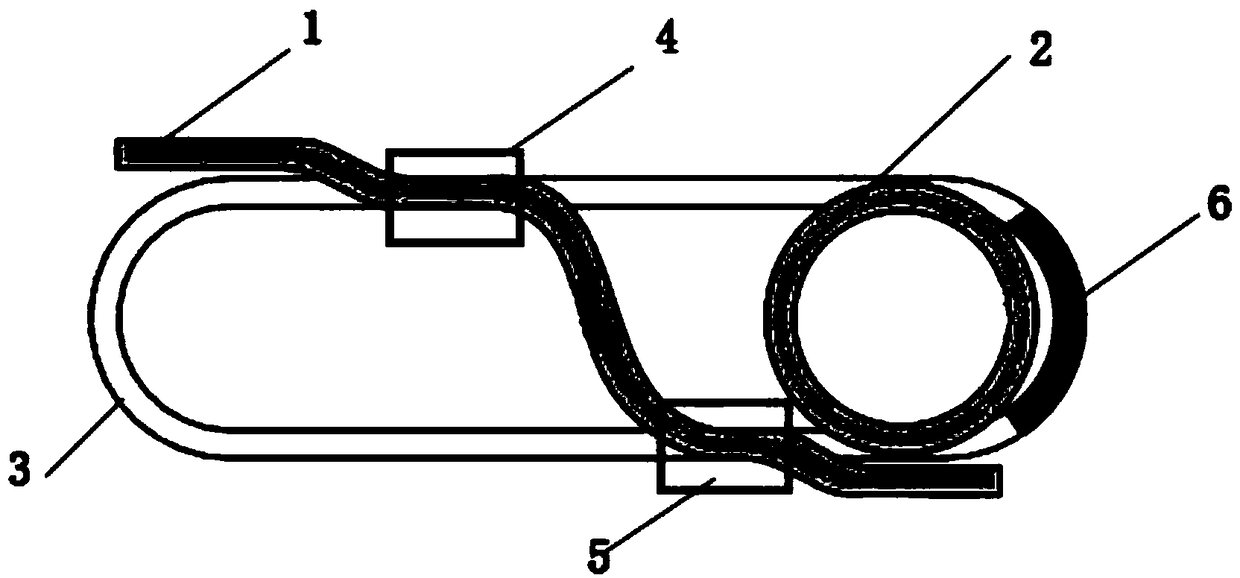
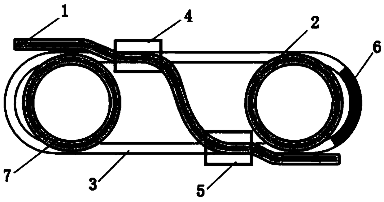
[0030] The following describes several preferred embodiments of the present invention with reference to the accompanying drawings, so as to make the technical content clearer and easier to understand. The present invention can be embodied in many different forms of embodiments, and the protection scope of the present invention is not limited to the embodiments mentioned herein.

[0031] In the drawings, components with the same structure are denoted by the same numerals, and components with similar structures or functions are denoted by similar numerals. The size and thickness of each component shown in the drawings are shown arbitrarily, and the present invention does not limit the size and thickness of each component. In order to make the illustration clearer, the thickness of parts is appropriately exaggerated in some places in the drawings.

[0032] Such as figure 1 As shown, the present invention provides a specific embodiment of a curved waveguide assembly of a single ...


PUM


Abstract

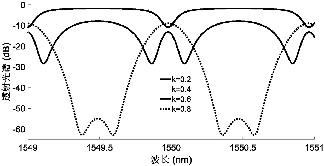
The invention discloses a silicon-nitride three-dimensional integrated multi-micro-cavity resonant filter, and the filter comprises a feedback waveguide which is coated with silicon dioxide and is located at the upper layer, an integrated sub-micro-ring structure, and a micro-ring resonant cavity located at the bottom layer, wherein the feedback waveguide at the upper layer interacts with the micro-ring resonant cavity at the bottom layer, so as to divide the light of the same light source into two beams in a device and enable the two beams to be resonant for output at an output port, therebyobtaining a compact filtering effect. A metal heating electrode is attached above the micro-ring resonant cavity, thereby achieving the switching of the amplitude modulation of a loaded electric signal to the phase modulation of an optical signal. The invention also discloses a preparation method for the silicon-nitride three-dimensional integrated multi-micro-cavity resonant filter. A three-dimensional vertical integrated design enables chips to be integrated more compactly, and reduces the insertion loss of an optical waveguide. The manufacturing technology is compatible with the semiconductor processing technology. The modulation efficiency is high, and the energy consumption is low. The filter can be produced in batch at low cost, and the filter is good in application prospect in the field of optical signal processing.

Description

technical field [0001] The invention relates to the field of tunable optical filters, in particular to a silicon nitride three-dimensional integrated multi-microcavity resonant filter device and a preparation method thereof. Background technique [0002] With the advent of the era of big data, the bandwidth and capacity of communication networks are increasing rapidly. Based on the existing traditional optical signal processing devices, not only the bandwidth and speed encounter bottlenecks, but the energy consumed also increases sharply. Therefore, it is urgent to develop ultra-high-speed low-energy new integrated optoelectronic devices. Among them, the optical modulator, as a core device in many fields such as optical information processing, spectral measurement, and optical storage, has developed a variety of devices based on effects such as electro-optic, acousto-optic, and magneto-optical effects. Regulating the amplitude or phase of the output light has certain advant...

Claims


Application Information

Patent Timeline
Patent Type & Authority Applications(China)
IPC IPC(8): G02B6/293
CPCG02B6/29337G02B6/29338G02B6/2934
Inventor 冯吉军翟珊张福领封治华曾和平
Owner UNIV OF SHANGHAI FOR SCI & TECH
Learn More