All-carbon memristor and preparation method thereof
A memristor and graphene technology, applied in electrical components and other directions, can solve the problems of complex preparation process, difficult industrial production, harsh preparation conditions, etc., and achieve the effects of simple preparation process, stable performance and good conductivity
- Summary
- Abstract
- Description
- Claims
- Application Information
AI Technical Summary
Problems solved by technology
Method used
Image
Examples
Embodiment 1
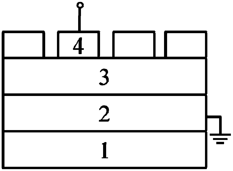
[0045] The preparation method of the all-carbon memristor of this embodiment is as follows:
[0046] (1) Provide a substrate and pretreat the substrate: the substrate in this embodiment is a glass slide, which is an insulating substrate. The substrate was ultrasonically treated with acetone for 30 minutes, and dried with nitrogen gas to remove surface impurities and dust substances.
[0047] (2) Transfer the bottom electrode layer on the substrate by vacuum filtration: get acetone and dissolve it in deionized water, the mass fraction of acetone is about 75%, to form an acetone aqueous solution, and add high-purity flake graphite powder to the acetone aqueous solution to obtain 3mg / ml of graphite dispersion, the graphite dispersion is placed in an ultrasonic cleaning machine to vibrate for 1h to obtain a graphene dispersion containing graphene, take it out and let it stand for 24h, then carry out the graphene dispersion containing graphene at 1000rpm, 4h Centrifuge to obtain ...
Embodiment 2
[0055] The difference with Example 1 is only that the graphene oxide solution taken in step (3) is 0.6ml, and vacuum filtration is carried out after being diluted to 100ml. After the transfer, the thickness of the graphene oxide intermediate dielectric layer is about 30nm.
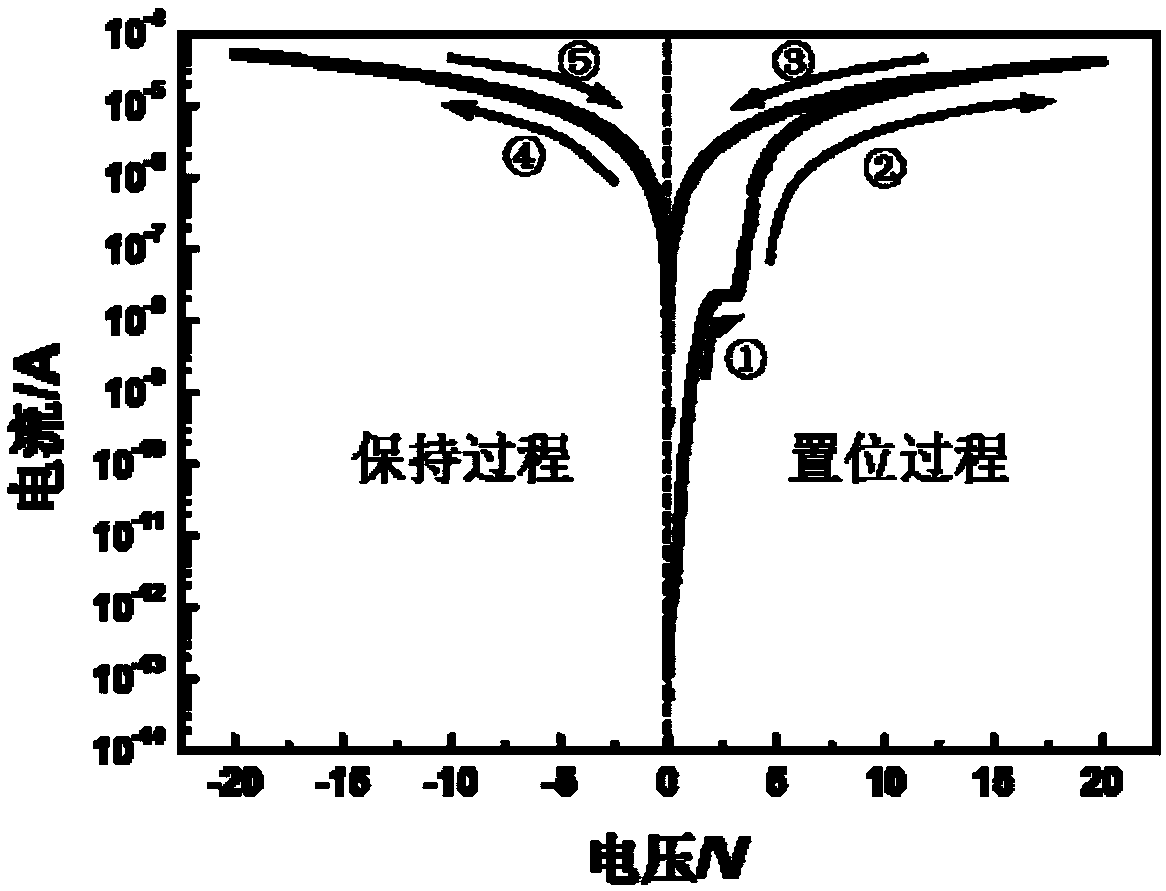
[0056] The electrical properties of the memristor prepared in this embodiment were tested. During the test, the bottom electrode was grounded and the top electrode was applied with voltage. Its current-voltage characteristic curve is as follows Figure 4 As shown, it can be seen from the figure that the characteristic curve of the device includes two parts: one part is the setting process, and the other part is the reset process. It can be seen that the device realizes the transformation of resistance.
Embodiment 3
[0058] The difference with Example 1 is only that the graphene dispersion liquid taken in the step (2) is 20ml, and vacuum filtration is carried out after being diluted to 100ml. After transfer, its graphene bottom electrode thickness is about 260nm. The current-voltage characteristic curve of the memristor prepared in this embodiment is as follows Figure 5 shown.
PUM
| Property | Measurement | Unit |
|---|---|---|
| thickness | aaaaa | aaaaa |
| thickness | aaaaa | aaaaa |
| thickness | aaaaa | aaaaa |
Abstract
Description
Claims
Application Information
 - R&D
- Intellectual Property
- Life Sciences
- Materials
- Tech Scout
- Unparalleled Data Quality
- Higher Quality Content
- 60% Fewer Hallucinations
Browse by: Latest US Patents, China's latest patents, Technical Efficacy Thesaurus, Application Domain, Technology Topic, Popular Technical Reports.
© 2025 PatSnap. All rights reserved.Legal|Privacy policy|Modern Slavery Act Transparency Statement|Sitemap|About US| Contact US: help@patsnap.com


