Aluminum nitride embedded PCB substrate and manufacturing method thereof

A technology of an aluminum nitride substrate and a manufacturing method, which is applied to the manufacture of printed circuits, the manufacture of printed circuit precursors, printed circuit components, etc. Low problems, to avoid environmental problems, prevent dents or fracturing, save steps for titanium removal

Inactive Publication Date: 2018-09-28
SHENZHEN KINWONG ELECTRONICS
View PDF6 Cites 5 Cited by
  • Summary
  • Abstract
  • Description
  • Claims
  • Application Information

AI Technical Summary

Problems solved by technology

At present, a few printed circuit board manufacturers have added aluminum nitride structures to printed circuit boards, but traditional aluminum nitride materials generally contain titanium, and at the same time, aluminum nitride is embedded in FR4 rigid substrates by manual operation. The efficiency is low, and there are hidden dangers in quality. In addition, it is necessary to use titanium removal solution for titanium removal treatment. The titanium removal solution contains hydrogen fluoride, which seriously pollutes the environment; there is also a large difference in thickness between aluminum nitride and FR4, which leads to depressions in the position of aluminum nitride or fracking problem

Method used


Image

  • Aluminum nitride embedded PCB substrate and manufacturing method thereof
  • Aluminum nitride embedded PCB substrate and manufacturing method thereof
  • Aluminum nitride embedded PCB substrate and manufacturing method thereof

Examples


Embodiment 1

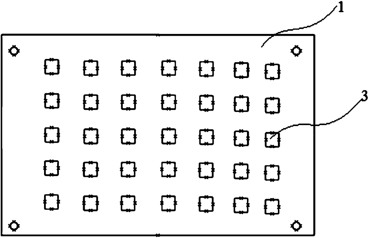
[0033] This embodiment provides an embedded aluminum nitride PCB substrate, such as Figure 1-2 As shown, the embedded aluminum nitride PCB substrate includes a rigid substrate 1, the rigid substrate 1 is an FR4 board, and the rigid substrate 1 is provided with a storage tank 2, and the storage tank 2 is provided with aluminum nitride Block 3, as shown in the figure, the bottom surface of the aluminum nitride block 3 is attached to the bottom surface of the storage tank 2, and the height difference between the top surface of the aluminum nitride block 3 and the top surface of the rigid substrate 1 is not more than 20 μm. It is convenient to assemble the aluminum nitride block 3 , and the distance between the aluminum nitride block 3 and the inner sidewall of the accommodating groove 2 is 50 μm.

[0034] Further, the top surface and the bottom surface of the aluminum nitride block 3 are sequentially provided with a conductive layer 4 and a copper plating layer 5 along a directi...

Embodiment 2

[0036] This embodiment provides an embedded aluminum nitride PCB substrate, such as Figure 1-2 As shown, the embedded aluminum nitride PCB substrate includes a rigid substrate 1, the rigid substrate 1 is an FR4 board, and the rigid substrate 1 is provided with a storage tank 2, and the storage tank 2 is provided with aluminum nitride Block 3, as shown in the figure, the bottom surface of the aluminum nitride block 3 is attached to the bottom surface of the storage tank 2, and the height difference between the top surface of the aluminum nitride block 3 and the top surface of the rigid substrate 1 is not more than 20 μm. It is convenient to assemble the aluminum nitride block 3 , and the distance between the aluminum nitride block 3 and the inner sidewall of the accommodating groove 2 is 100 μm.

[0037] Further, the top surface and the bottom surface of the aluminum nitride block 3 are sequentially provided with a conductive layer 4 and a copper plating layer 5 along the dire...

Embodiment 3

[0039] This embodiment provides an embedded aluminum nitride PCB substrate, such as Figure 1-2As shown, the embedded aluminum nitride PCB substrate includes a rigid substrate 1, the rigid substrate 1 is an FR4 board, and the rigid substrate 1 is provided with a storage tank 2, and the storage tank 2 is provided with aluminum nitride Block 3, as shown in the figure, the bottom surface of the aluminum nitride block 3 is attached to the bottom surface of the storage tank 2, and the height difference between the top surface of the aluminum nitride block 3 and the top surface of the rigid substrate 1 is not more than 20 μm. It is convenient to assemble the aluminum nitride block 3 , and the distance between the aluminum nitride block 3 and the inner sidewall of the accommodating groove 2 is 80 μm.

[0040] Further, the top surface and the bottom surface of the aluminum nitride block 3 are sequentially provided with a conductive layer 4 and a copper plating layer 5 along a directio...


PUM

PropertyMeasurementUnit
thicknessaaaaaaaaaa
thicknessaaaaaaaaaa
widthaaaaaaaaaa

Abstract

The invention discloses an aluminum nitride embedded PCB substrate comprising a rigid substrate in which an accommodating groove is formed, an aluminum nitride block is arranged in the accommodating groove, a conductive layer and a copper planted layer are successively arranged on the top surface and the bottom surface of the aluminum nitride block along directions far away from the aluminum nitride block. As the aluminum nitride block has high thermal conductivity, low dielectric constant, low dielectric loss and excellent electrical insulating property, the heat dissipation performance of the rigid substrate is significantly improved, the aluminum nitride block substrate does not include titanium, the step of removing the titanium is saved, the manufacturing process of the substrate is shortened, and meanwhile the environment problem caused by titanium removing solution is also avoided. The invention also discloses a method for manufacturing the aluminum nitride embedded PCB substrate, with high laser cutting accuracy and efficiency. The mode of using a mechanical arm for automatically grasping the aluminum nitride block and placing the aluminum nitride block into the accommodating groove is used for embedding the aluminum nitride block; compared with the conventional manual taking and placing operations, the mode of the manufacturing method provided by the invention is significantly improved in machining efficiency, operation staffs are also prevented from directly contacting the aluminum nitride block and polluting the same, and thus the hidden quality troubles are reduced.

Description

technical field [0001] The invention belongs to the technical field of printed circuit board production, and in particular relates to a printed circuit board substrate embedded with aluminum nitride and a manufacturing method thereof. Background technique [0002] With the rapid development of integration technology and microelectronic packaging technology, the total power density of electronic components is increasing, while the physical size of electronic components and electronic equipment is gradually becoming smaller and miniaturized, and the heat generated by electronic components is rapidly increasing. Accumulation leads to an increase in heat flux near integrated devices, forming a high-temperature environment, and excessive temperature reduces the performance and service life of electronic components and equipment. The heat dissipation performance of printed circuit boards used to provide mechanical support for fixing and assembling electronic components and to real...

Claims


Application Information

Patent Timeline
Patent Type & Authority Applications(China)
IPC IPC(8): H05K1/02H05K3/02
CPCH05K1/0201H05K3/022
Inventor 侯利娟付凤奇马奕
Owner SHENZHEN KINWONG ELECTRONICS
Why Eureka
Try Eureka