Pixel circuit and display device
A pixel circuit and electrode technology, which is applied in the field of organic light-emitting display, can solve the problems of light-emitting diode current difference and uneven light emission of display devices, and achieve the effects of avoiding insufficient brightness, eliminating uneven light emission, and improving the uniformity of light emission
- Summary
- Abstract
- Description
- Claims
- Application Information
AI Technical Summary
Problems solved by technology
Method used
Image

Examples
Embodiment 1
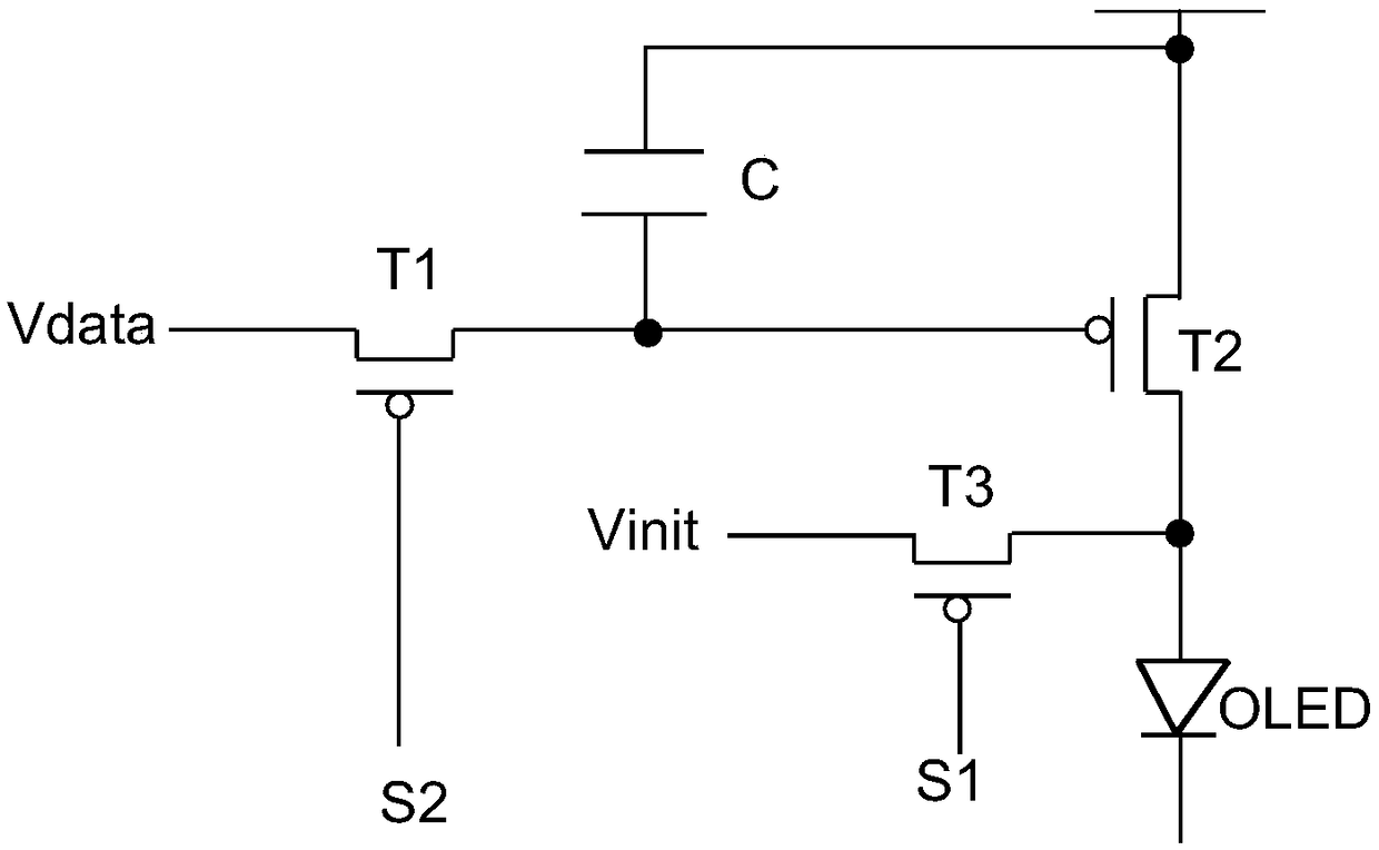
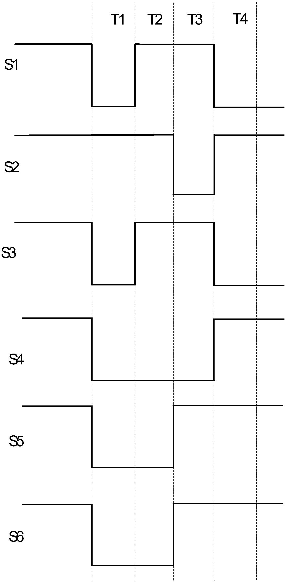
[0031] combine Figure 2-7 As shown, a detailed description of a pixel circuit provided in Embodiment 1 of the present application is given, referring to figure 2 As shown, it is a schematic structural diagram of a pixel circuit provided in Embodiment 1 of the present application, wherein the pixel circuit is used to drive the light-emitting element OLED, and the light-emitting element OLED is a light-emitting diode, and the pixel circuit includes:
[0032] The first transistor M1, the second transistor M2, the third transistor M3, the fourth transistor M4, the fifth transistor M5, the sixth transistor M6, the driving transistor M0, the first capacitor C1 and the second capacitor C2;
[0033] The gate of the first transistor M1 is connected to the first driving signal S1, the first electrode of the first transistor M1 is connected to the anode voltage Vpvdd, and the second electrode of the first transistor M1 is connected to the driving signal S1. the source of transistor M0...
Embodiment 2
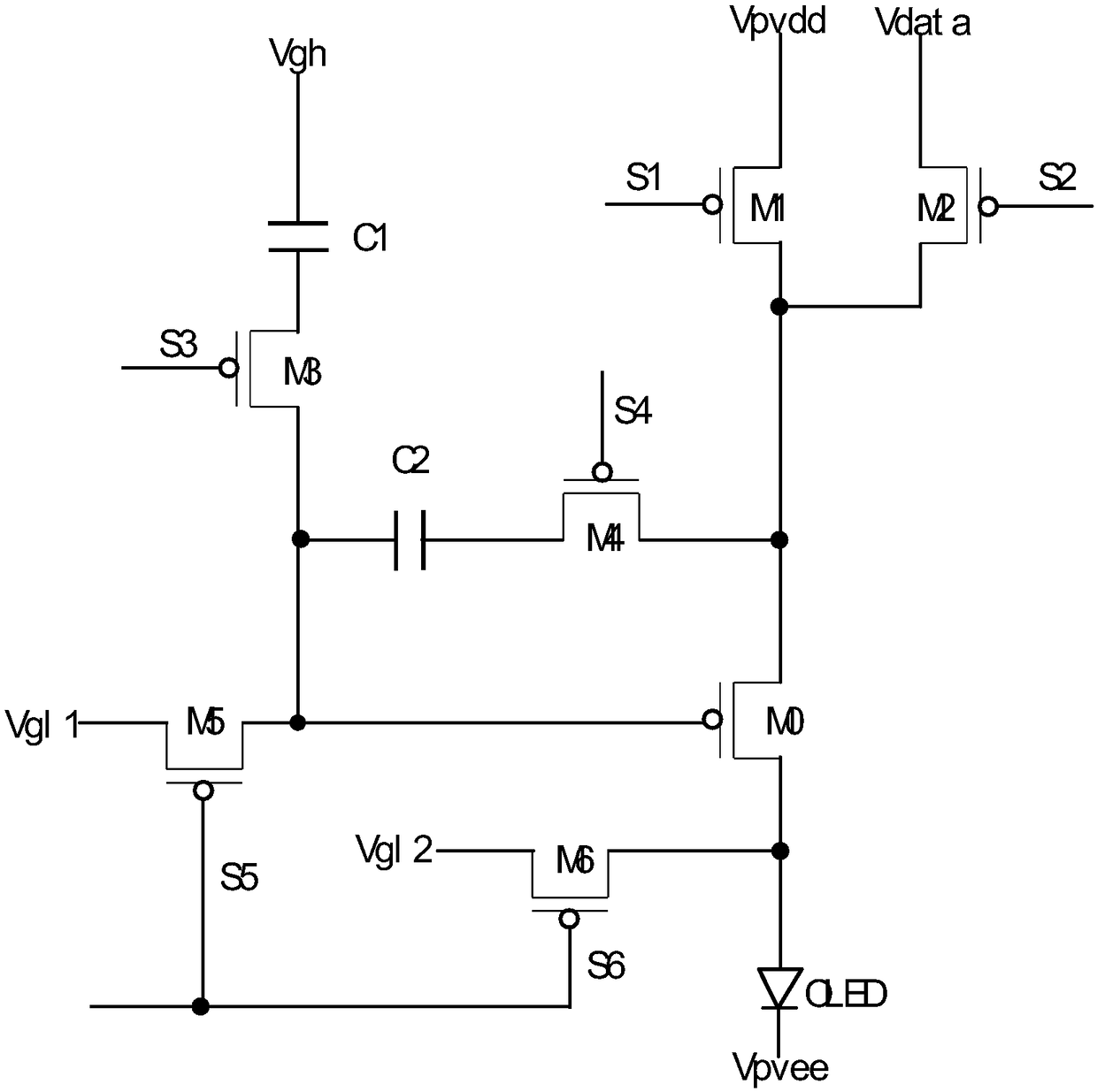
[0069] combine Figure 9 and 10 As shown, a pixel circuit provided in Embodiment 2 of the present application is described in detail, and reference Figure 9 As shown, it is a schematic structural diagram of a pixel circuit provided in Embodiment 2 of the present application, wherein the pixel circuit is used to drive the light-emitting element OLED, the light-emitting element OLED is a light-emitting diode, and the pixel circuit includes:
[0070] The first transistor M1, the second transistor M2, the third transistor M3, the fourth transistor M4, the fifth transistor M5, the sixth transistor M6, the driving transistor M0, the first capacitor C1 and the second capacitor C2;
[0071] The gate of the first transistor M1 is connected to the first driving signal S1, the first electrode of the first transistor M1 is connected to the anode voltage Vpvdd, and the second electrode of the first transistor M1 is connected to the driving signal S1. the source of transistor M0;
[007...
PUM
 Abstract
Description
Claims
Application Information
 - R&D
- Intellectual Property
- Life Sciences
- Materials
- Tech Scout
- Unparalleled Data Quality
- Higher Quality Content
- 60% Fewer Hallucinations
Browse by: Latest US Patents, China's latest patents, Technical Efficacy Thesaurus, Application Domain, Technology Topic, Popular Technical Reports.
© 2025 PatSnap. All rights reserved.Legal|Privacy policy|Modern Slavery Act Transparency Statement|Sitemap|About US| Contact US: help@patsnap.com