OLED pixel driving circuit, OLED display panel and driving method

A pixel driving circuit and driving method technology, applied in static indicators, instruments, etc., can solve problems such as inability to eliminate drift voltage, insufficient charge and discharge time, and large variable voltage difference, so as to improve display quality and eliminate uneven luminescence Effect

Active Publication Date: 2019-12-03
SHENZHEN CHINA STAR OPTOELECTRONICS SEMICON DISPLAY TECH CO LTD
View PDF8 Cites 0 Cited by
  • Summary
  • Abstract
  • Description
  • Claims
  • Application Information

AI Technical Summary

Problems solved by technology

However, the above existing 5T1C pixel driving circuit driving methods have the following disadvantages: the voltage at VDD needs to be changed, the change is fast and the voltage difference is large, the charging and discharging time is insufficient, and the current is too large; the hardware required to change the voltage at VDD is relatively complicated, and The driving transistor here should be a P-type transistor, otherwise the drift voltage cannot be eliminated
like figure 1 As shown, in the existing OLED 2T1C pixel driving circuit, after the Gate is turned on, the Vdata potential is stored in the capacitor Cst, and the driving TFT remains on, so that the OLED is always in a DC bias state. This driving method is likely to cause aging of the OLED
like Figure 2a and Figure 2b As shown, the existing OLED 5T1C pixel drive circuit OLED does not normally eliminate the threshold voltage and the operation of changing VDD is difficult to achieve

Method used


Image

  • OLED pixel driving circuit, OLED display panel and driving method
  • OLED pixel driving circuit, OLED display panel and driving method
  • OLED pixel driving circuit, OLED display panel and driving method

Examples


Embodiment Construction

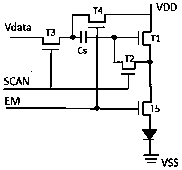
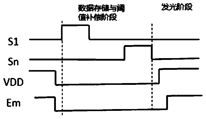
[0040] see image 3 and Figure 4 , image 3 It is a schematic circuit diagram of a preferred embodiment of the OLED pixel driving circuit of the present invention, Figure 4 for image 3 Timing diagram of the circuit shown. The present invention proposes a 5T2C OLED pixel circuit for driving organic light-emitting diodes. The circuit of this preferred embodiment mainly includes:

[0041] The thin film transistor T1 has its gate connected to node C, its source and drain connected to node B and node A respectively; the thin film transistor T2 has its gate connected to the scan signal Scan, its source and drain connected to node A and node C respectively; The gate of the transistor T3 is connected to the scanning signal Scan, the source and the drain are respectively connected to the node B and the input data voltage Vdata; the gate of the thin film transistor T4 is connected to the light emitting signal EM, and the source and the drain are respectively connected to the node...


PUM


Abstract

An OLED pixel driving circuit, an OLED display panel, and a driving method. The driving circuit is characterized in that: a gate of a first thin-film transistor (T1) is connected to a third node (C), and a source and a drain of the first thin-film transistor (T1) are correspondingly connected to a second node (B) and a first node (A). A gate of a second thin-film transistor (T2) is connected to a scanning signal (SCAN), and a source and a drain of the second thin-film transistor (T2) are correspondingly connected to the first node (A) and the third node (C). A gate of a third thin-film transistor (T3) is connected to a scanning signal (SCAN), and a source and a drain of the third thin-film transistor (T3) are correspondingly connected to the second node (B) and an input data voltage (Vdata). A gate of a fourth thin-film transistor (T4) is connected to a light-emitting signal (EM),and a source and a drain of the fourth thin-film transistor (T4) are correspondingly connected to the second node (B) and a direct-current high voltage (VDD). A gate of a fifth thin-film transistor (T5) is connected to a light-emitting signal (EM), and a source and a drain of the fifth thin-film transistor (T5) are correspondingly connected to the first node (A) and an anode of an OLED. A first capacitor (C1) and a second capacitor (C2). By means of the driving circuit and the driving method, the phenomenon of uneven light emission caused by the process of the driving transistors is eliminated.

Description

technical field [0001] The invention relates to the field of display technology, in particular to an OLED pixel driving circuit, an OLED display panel and a driving method. Background technique [0002] As a new generation of display technology, organic light-emitting diode (OLED) display panels have the advantages of low power consumption, high color gamut, high brightness, high resolution, wide viewing angle, and high response speed, so they are favored by the market. [0003] According to the driving method, OLED display devices can be divided into two categories: passive matrix OLED (Passive Matrix OLED, PMOLED) and active matrix OLED (Active Matrix OLED, AMOLED). Among them, AMOLED has pixels arranged in an array, belongs to the active display type, has high luminous efficiency, and is usually used as a high-definition large-size display device. [0004] see figure 1 , which is a schematic diagram of an existing OLED 2T1C pixel drive circuit, the existing drive method...

Claims


Application Information

Patent Timeline
Patent Type & Authority Patents(China)
IPC IPC(8): G09G3/3258
CPCG09G3/3258G09G2320/0233
Inventor 王珊陈小龙
Owner SHENZHEN CHINA STAR OPTOELECTRONICS SEMICON DISPLAY TECH CO LTD
Why Eureka
Try Eureka