Method for preparing two-dimensional sheet-shaped Cu-MOF (Metal Organic Framework) material
A flake, cu-btc technology, applied in carboxylate preparation, organic chemistry methods, chemical instruments and methods, etc., can solve the problems of low yield, limit the promotion and application of two-dimensional MOF materials, harsh conditions, etc., and achieve catalytic The effect of high activity, high yield and mild reaction conditions
- Summary
- Abstract
- Description
- Claims
- Application Information
AI Technical Summary
Problems solved by technology
Method used
Image
Examples
Embodiment 1
[0027] Mix Cu-BTC and urea solution with pH=9 at a solid-to-liquid ratio of 1 / 100g / ml, stir at 25°C for 5 hours, filter, wash, and dry to obtain a two-dimensional sheet-like Cu-MOF-25 with a thickness of 30nm ~ 100nm. In the catalytic oxidation experiment of styrene, the conversion rate reached 98.97% when reacting for 5 hours.
Embodiment 2
[0029] Mix Cu-BTC and sodium hydroxide solution with pH=10 at a solid-to-liquid ratio of 1 / 80g / ml, stir at 80°C for 2 hours, filter, wash, and dry to obtain two-dimensional flaky Cu-MOF-80, which The thickness is 200nm-300nm. In the catalytic oxidation experiment of styrene, the conversion rate reached 97.42% when reacting for 5 hours.
Embodiment 3
[0031] Mix Cu-BTC and ammonia aqueous solution with pH=12 at a solid-to-liquid ratio of 1 / 50g / ml, stir at 120°C for 1 hour, filter, wash, and dry to obtain two-dimensional sheet-like Cu-MOF-120 with a thickness of 400nm ~ 500nm. In the catalytic oxidation experiment of styrene, the conversion rate reaches 97.15% when reacting for 5 hours.
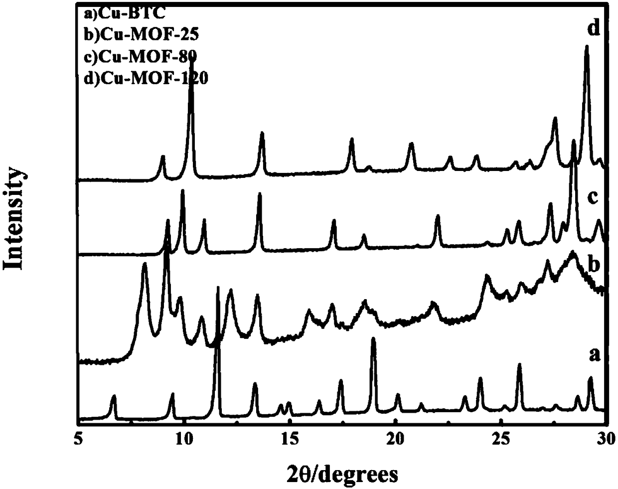
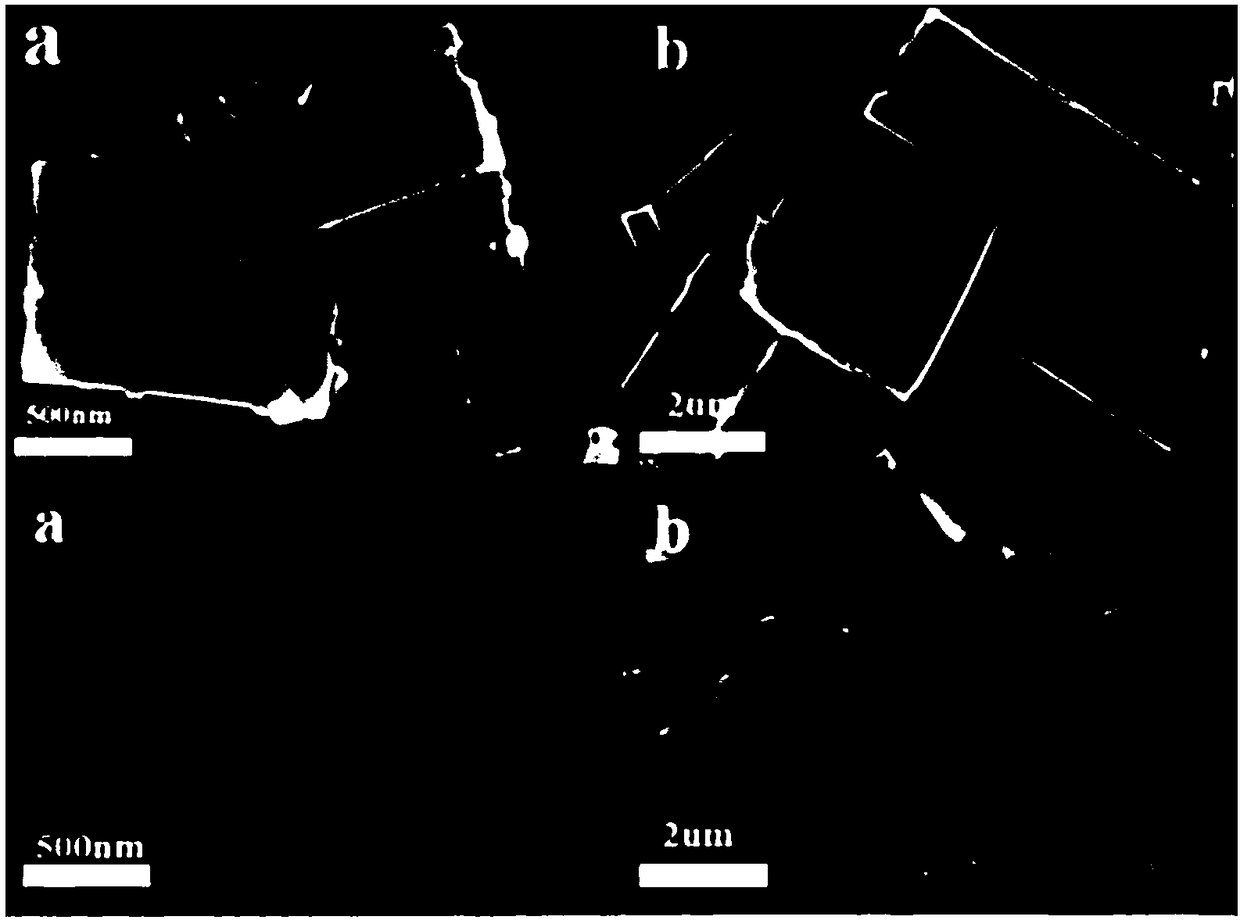
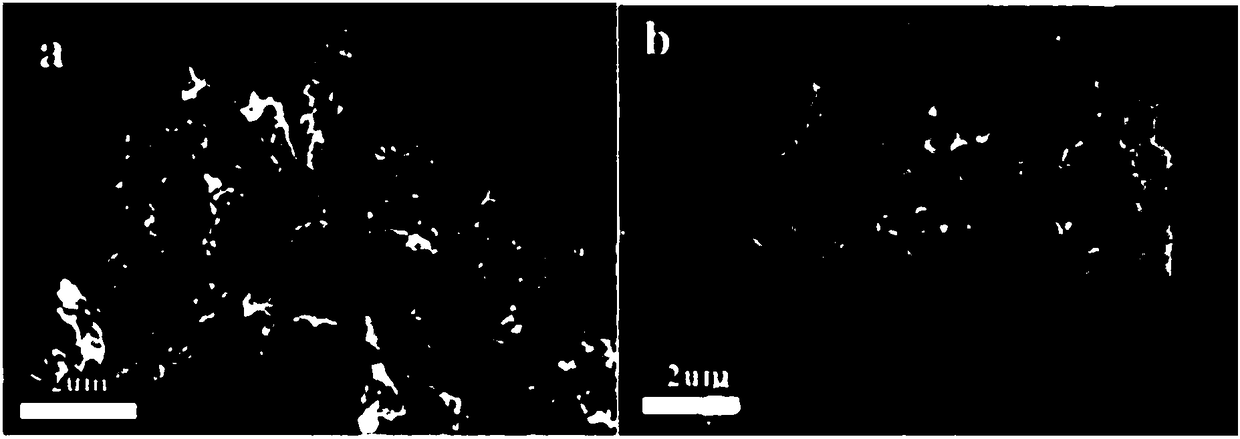
[0032] In the above examples, the XRD comparison diagram of the crystal structure before and after Cu-BTC transformation is as follows figure 1 Wherein a) is Cu-BTC before transformation, b) is the XRD pattern of Cu-MOF after transformation at 25°C in Example 1, and c) is Cu-MOF after transformation at 80°C in Example 2 d) is the XRD pattern of Cu-MOF transformed at 120°C in Example 3. Scanning electron micrographs (SEM) of the transformed crystal morphology as figure 2 Shown, where a is the SEM image of the Cu-MOF transformed at 25°C in Example 1, and b is the SEM image of the Cu-MOF transformed at 80°C in Example 2.
PUM
 Abstract
Description
Claims
Application Information
 - R&D Engineer
- R&D Manager
- IP Professional
- Industry Leading Data Capabilities
- Powerful AI technology
- Patent DNA Extraction
Browse by: Latest US Patents, China's latest patents, Technical Efficacy Thesaurus, Application Domain, Technology Topic, Popular Technical Reports.
© 2024 PatSnap. All rights reserved.Legal|Privacy policy|Modern Slavery Act Transparency Statement|Sitemap|About US| Contact US: help@patsnap.com


