How to make oled display panel

A technology of display panel and supporting bottom plate, which is applied in semiconductor/solid-state device manufacturing, semiconductor devices, electrical components, etc., and can solve problems such as inferior OLED display panel quality

Active Publication Date: 2020-10-27
WUHAN CHINA STAR OPTOELECTRONICS SEMICON DISPLAY TECH CO LTD
View PDF9 Cites 0 Cited by
  • Summary
  • Abstract
  • Description
  • Claims
  • Application Information

AI Technical Summary

Problems solved by technology

[0005] The purpose of the present invention is to provide a method for manufacturing OLED display panels to solve the technical problems of poor OLED display panel quality caused by laser lift-off technology in the prior art

Method used


Image

  • How to make oled display panel
  • How to make oled display panel
  • How to make oled display panel

Examples


Embodiment Construction

[0028] The following descriptions of the various embodiments refer to the accompanying drawings to illustrate specific embodiments in which the present invention can be practiced. The directional terms mentioned in the present invention, such as "up", "down", "front", "back", "left", "right", "inside", "outside", "side", etc., are for reference only The orientation of the attached schema. Therefore, the directional terms used are used to illustrate and understand the present invention, but not to limit the present invention. In the figures, structurally similar units are denoted by the same reference numerals.

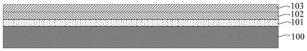
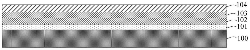
[0029] Please refer to Figures 1A to 1F , Figures 1A to 1F It is a schematic flowchart of a method for manufacturing an OLED display panel according to a preferred embodiment of the present invention. The method includes the following steps.

[0030] First, if Figure 1A As shown, a support base 100 is provided. Specifically, the supporting bottom plate 100 is a...


PUM

PropertyMeasurementUnit
wavelengthaaaaaaaaaa

Abstract

The invention provides a method for manufacturing an OLED display panel. The method comprises the steps of: providing a support base; forming a substrate layer on the support base; forming a buffer layer on the substrate layer; forming a flexible polymer layer on the buffer layer; forming an OLED array layer on the flexible polymer layer; and using a laser to heat the support base to decompose the buffer layer, thereby separating the substrate layer from the flexible polymer layer.

Description

【Technical field】 [0001] The invention relates to the field of organic light emitting diode panels, in particular to a method for manufacturing an OLED display panel. 【Background technique】 [0002] Among flat panel display technologies, Organic Light-Emitting Diode (OLED) displays have many advantages such as thinness, active light emission, fast response speed, large viewing angle, wide color gamut, high brightness and low power consumption, etc., and have gradually become a new trend. A generation of display technology. [0003] In the manufacturing process of OLED display panels, laser lift-off (laser lift-off, LLO) is the step of separating the glass substrate from the flexible polyimide (PI) layer by using laser, in which the laser will destroy the glass and polyimide. Hydrogen bonding forces between the imide layers to achieve effective separation between the glass and polyimide layers. However, if the energy of the laser is too low, the polyimide layer and the glas...

Claims


Application Information

Patent Timeline
Patent Type & Authority Patents(China)
IPC IPC(8): H01L51/56H01L51/00
CPCH10K71/80H10K71/00
Inventor 袁朝煜王超梁
Owner WUHAN CHINA STAR OPTOELECTRONICS SEMICON DISPLAY TECH CO LTD
Why Eureka
Try Eureka