Surface-mounted support and multi-chip photoelectric device

A mounting type, conductive substrate technology, applied in the direction of electrical solid devices, electrical components, semiconductor devices, etc., can solve the problems of weak bonding force of insulating materials, poor heat dissipation effect, and difficulty in achieving low voltage, etc., to achieve the realization of solid crystal bonding wire Design, low bonding wire design, the effect of realizing voltage

Active Publication Date: 2018-09-14
KAISTAR LIGHTING (XIAMEN) CO LTD
View PDF9 Cites 0 Cited by
  • Summary
  • Abstract
  • Description
  • Claims
  • Application Information

AI Technical Summary

Problems solved by technology

The current mounting process is to use solder paste for reflow soldering, and in reflow soldering, the void rate may be too large due to pad design, improper reflow soldering curve, etc., and too large void rate will easily lead to poor heat dissipation
Furthermore, the larger the size of SMD (surface mount type) products, the larger the single die-bonding area and the larger number of chips in series, making it difficult to achieve low-voltage (such as 6V, etc.) designs
In addition, the bonding force between silica gel and metal materials and insulating materials is weak, and it is prone to delamination

Method used


Image

  • Surface-mounted support and multi-chip photoelectric device
  • Surface-mounted support and multi-chip photoelectric device
  • Surface-mounted support and multi-chip photoelectric device

Examples


no. 1 example

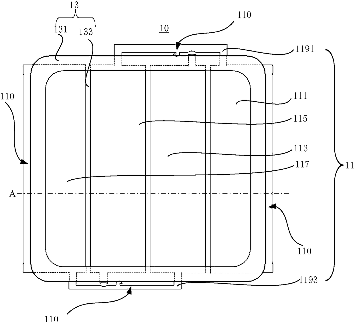
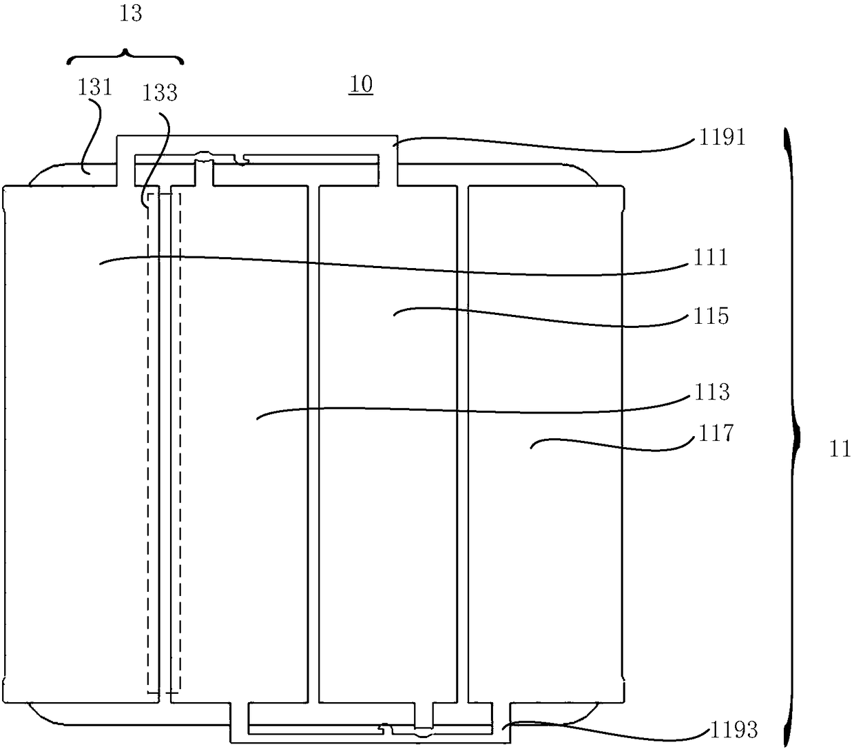
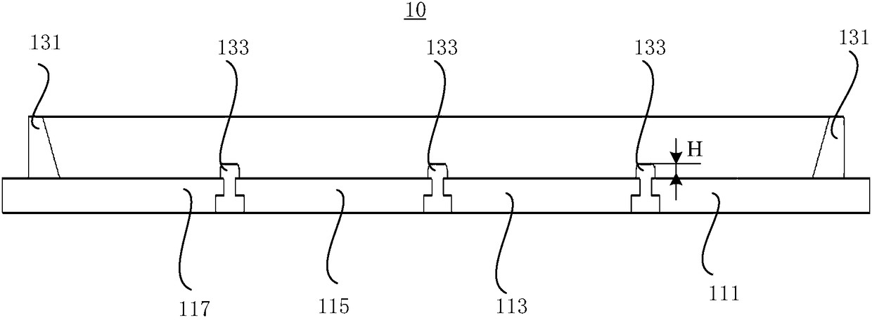
[0028] Such as Figure 1A , Figure 1B with Figure 1C As shown, a surface mount bracket 10 provided by the first embodiment of the present invention mainly includes: a conductive base 11 and an insulating material layer 13 .

[0029] Wherein, the conductive base 11 includes a plurality of connection pads, such as Figure 1A The shown connection pads 111 , 113 , 115 and 117 are arranged in a row and spaced from each other. The shape of the connection pad 111 , the connection pad 113 , the connection pad 115 and the connection pad 117 is substantially rectangular. The front surfaces of connection pad 111, connection pad 113, connection pad 115 and connection pad 117 (as Figure 1A shown) is used, for example, to form a die-bonding region, and the die-bonding region is used for disposing optoelectronic chips such as LED chips. And the back side of connection pad 111, connection pad 113, connection pad 115 and connection pad 117 (such as Figure 1B shown) is used, for example,...

no. 2 example

[0045] Such as figure 2 As shown, a multi-chip optoelectronic device 20 provided by the second embodiment of the present invention mainly includes: a plurality of optoelectronic chips such as a plurality of LED chips 23 and a surface mount bracket. Wherein, the surface mount bracket is, for example, the surface mount bracket 10 described in the aforementioned first embodiment, and its specific structure and function details can refer to the description of the aforementioned first embodiment, and will not be repeated here. A plurality of LED chips 23 are, for example, disposed in the die-bonding area of ​​the surface mount bracket.

[0046] The size of the surface mount bracket is, for example, 13mm*13mm. A plurality of LED chips 23 includes, for example, fifty-two or twenty-six pairs of LED chips 23. For example, the fifty-two LED chips 23 adopt "26 parallel and 2 strings", that is, two LEDs in each pair of LED chips 23 Chips are connected in series, and then twenty-six pai...


PUM

PropertyMeasurementUnit
Heightaaaaaaaaaa

Abstract

The embodiment of the invention discloses a surface-mounted support, and the support comprises a conductive substrate which comprises at least three connecting pads. The connecting pads are set at intervals, and the first surfaces of the connecting pads are used for forming a die bonding region. The second surfaces, opposite to the first surfaces, of the connecting pads are used for forming a bonding pad region. At least one of the connecting pads is positive, and the remaining connecting pads are negative. The support also comprises an insulating material layer which at least covers the firstsurface of the conductive substrate, surrounds the die bonding region and is disposed in the gaps between any two connecting pads. The embodiment of the invention also discloses a multi-chip photoelectric device which employs the support.

Description

technical field [0001] The invention relates to the field of optoelectronic technology, in particular to a surface mounting type bracket and a multi-chip optoelectronic device. Background technique [0002] At present, the size of SMD (Surface Mount Device, surface mount device) LED (Light-Emitting Diode, light-emitting diode) products is more and more diversified, and it is developing in the direction of large size. Power COB (Chip On Board, integrated chip) LED products. One of the characteristics of SMD products is that reflow soldering is required, and the LED chip is mounted on a conductive substrate for electrical connection and heat dissipation. The current mounting process is to use solder paste for reflow soldering. In reflow soldering, the void rate may be too large due to pad design, improper reflow soldering curve, etc., and too large void rate may easily lead to poor heat dissipation. Furthermore, the larger the size of the SMD type (surface mount type) produc...

Claims


Application Information

Patent Timeline
IPC IPC(8): H01L33/62H01L33/64H01L25/075
CPCH01L25/0753H01L33/62H01L33/64H01L2224/48137H01L23/49575H01L23/49861H01L33/486H01L23/49541H01L23/49503H01L23/49586H01L25/13
Inventor 张景琼
Owner KAISTAR LIGHTING (XIAMEN) CO LTD
Why Eureka
Try Eureka