A cutting device for photovoltaic panel silicon wafer processing

A cutting device and photovoltaic panel technology, which can be used in fine working devices, stone processing equipment, manufacturing tools, etc., can solve the problem of high cutting production costs

Active Publication Date: 2020-11-13
SHAOXING UNIVERSITY
View PDF9 Cites 0 Cited by
  • Summary
  • Abstract
  • Description
  • Claims
  • Application Information

AI Technical Summary

Problems solved by technology

[0004] Aiming at the deficiencies of the prior art, the present invention provides a cutting device for processing silicon wafers of photovoltaic panels, which solves the problem that the existing cutting devices for processing silicon wafers of photovoltaic panels have high production costs for cutting silicon wafers

Method used


Image

  • A cutting device for photovoltaic panel silicon wafer processing
  • A cutting device for photovoltaic panel silicon wafer processing
  • A cutting device for photovoltaic panel silicon wafer processing

Examples


Embodiment Construction

[0030] The following will clearly and completely describe the technical solutions in the embodiments of the present invention with reference to the accompanying drawings in the embodiments of the present invention. Obviously, the described embodiments are only some, not all, embodiments of the present invention. Based on the embodiments of the present invention, all other embodiments obtained by persons of ordinary skill in the art without making creative efforts belong to the protection scope of the present invention.

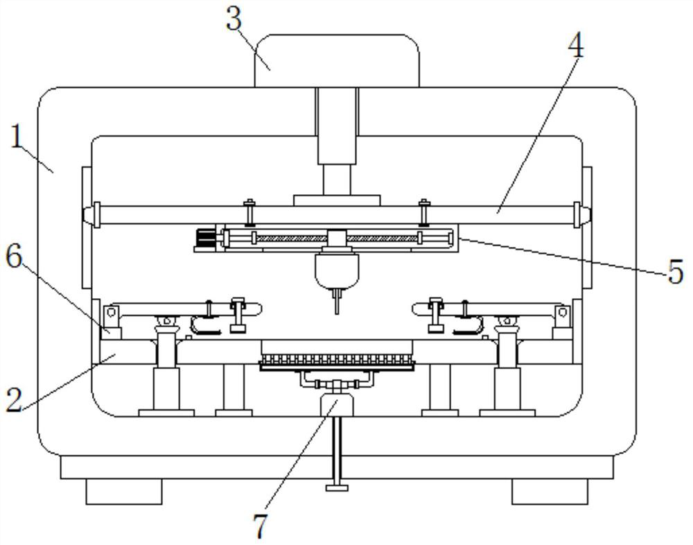
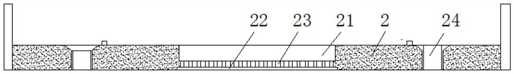
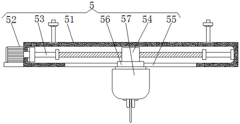
[0031] Such as Figure 1-7 As shown, the present invention provides a technical solution: a cutting device for processing silicon wafers of photovoltaic panels, including a body 1, the inner bottom of the body 1 is fixedly connected with a cutting table 2 through a support rod, and the middle position of the upper surface of the cutting table 2 is set Cutting groove 21 is arranged, and the bottom middle position of cutting table 2 is provided with connecting g...


PUM


Abstract

The invention relates to the technical field of photovoltaic equipment, and discloses a cutting device for processing silicon wafers of photovoltaic panels, which includes a body, the inner bottom of the body is fixedly connected to a cutting table through a support rod, and a hydraulic cylinder is fixedly connected to the middle position of the top of the body. The hydraulic telescopic rod of the cylinder runs through the top of the body and is fixedly connected with a load-bearing plate. The lower surface of the load-bearing plate is fixedly connected with a drive adjustment device. The cutting table is connected with two movable clamping devices. collection device. The invention solves the problem that the existing cutting device for processing silicon wafers of photovoltaic panels cannot perform good clamping and fixing when cutting silicon wafers by setting the body, the cutting table and the movable clamping device to cooperate with each other. The cutting table, hydraulic cylinder, bearing plate, drive adjustment device, movable clamping device and purification collection device cooperate with each other to effectively improve the performance of the silicon wafer cutting device.

Description

technical field [0001] The invention relates to the technical field of photovoltaic equipment, in particular to a cutting device for processing silicon wafers of photovoltaic panels. Background technique [0002] With the development of new energy, the application of photovoltaic equipment has been greatly popularized. The photovoltaic panel silicon wafers of photovoltaic equipment need to be cut according to specific production needs during processing, but the existing cutting device for photovoltaic panel silicon wafer processing Good clamping and fixing cannot be carried out when cutting silicon wafers, resulting in damage to silicon wafers during clamping, which reduces the yield of products. The lateral feed error during cutting is large, resulting in a large error in silicon wafer cutting, resulting in high production costs for silicon wafers, and at the same time, the debris generated during silicon wafer cutting cannot be effectively recycled and reused, which affect...

Claims


Application Information

Patent Timeline
Patent Type & Authority Patents(China)
IPC IPC(8): B28D5/04B28D7/00B28D7/02B28D7/04
CPCB28D5/0058B28D5/0076B28D5/0082B28D5/045
Inventor 刘士彦
Owner SHAOXING UNIVERSITY
Why Eureka
Try Eureka