
Microstructural on-chip light source device based on straight waveguide total reflection coupling connection and production method of microstructural on-chip light source device

A technology of coupling connection and light source device, applied in the field of microstructure on-chip light source device based on straight waveguide total reflection coupling connection, can solve the problems of incompatibility with CMOS large-scale integration standard process, inability to lasing, low power, etc. Controlled optical power output, low-loss loop oscillation, and low-cost effects

Pending Publication Date: 2018-09-11
JIANGSU HUAXING LASER TECH CO LTD
View PDF14 Cites 0 Cited by
  • Summary
  • Abstract
  • Description
  • Claims
  • Application Information

AI Technical Summary

Problems solved by technology

[0003] Optoelectronic integration is currently mainly concentrated in four systems, namely: III-V system, lithium niobate system, silicon dioxide system and silicon-based system, each with its own advantages and disadvantages; the first three developed earlier and have more applications. However, it is not compatible with the CMOS large-scale integration standard process, which limits its integration with microelectronics. Silicon-based integration is compatible with CMOS processes, but there is currently no better way to solve the problem for silicon-based lasers; The III-V group realizes light emission, and then couples into the silicon-based waveguide through the evanescent field or mode spot matching;
[0004] Since most of III-V materials are direct bandgap materials and have high radiative transition rates, they are very suitable as light-emitting materials, especially quantum well and quantum dot structures, which can realize artificial tailoring of semiconductor materials and greatly improve device performance; usually The laser structure includes: FP straight cavity structure, distributed feedback (DFB) structure, distributed reflection (DBR) structure, ring cavity structure and various micro cavity structures; these structures can be used as independent devices or as on-chip integrated light sources , especially ring cavities and microcavities are more common; however, the characteristics of these structures limit their volume and power. Working in the whispering gallery mode, the power is very small and difficult to detect;

Method used


Image

  • Microstructural on-chip light source device based on straight waveguide total reflection coupling connection and production method of microstructural on-chip light source device
  • Microstructural on-chip light source device based on straight waveguide total reflection coupling connection and production method of microstructural on-chip light source device
  • Microstructural on-chip light source device based on straight waveguide total reflection coupling connection and production method of microstructural on-chip light source device

Examples


Embodiment Construction

[0031] In order to make the object, technical solution and advantages of the present invention clearer, the present invention will be further described in detail below in conjunction with the accompanying drawings and specific embodiments. It should be understood that the specific embodiments described here are only used to explain the present invention, not to limit the present invention.

[0032] In the following text, many aspects of the invention will be better understood with reference to the accompanying drawings. Components in the figures are not necessarily drawn to scale. Instead, emphasis is placed on clearly illustrating the components of the invention. Furthermore, like reference numerals indicate corresponding parts throughout the several views of the drawings.

[0033] As used herein, the word "exemplary" or "illustrative" means serving as an example, instance, or illustration. Any implementation described herein as "exemplary" or "illustrative" is not necessa...


PUM


Abstract

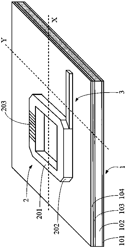
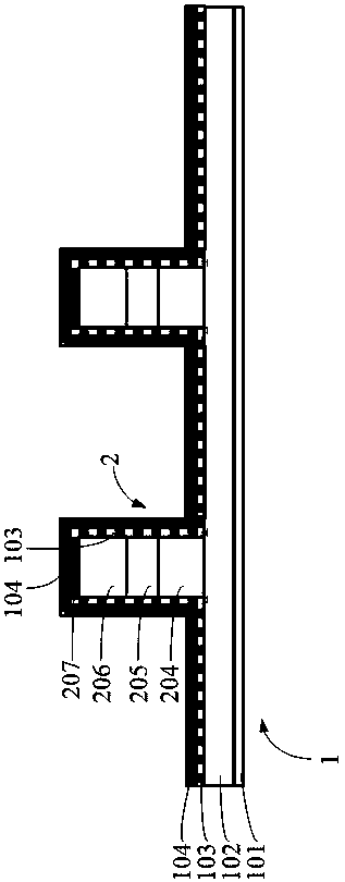
The invention relates to technical field of design of photoelectronic devices and particularly relates to a microstructural on-chip light source device based on straight waveguide total reflection coupling connection and a production method of the microstructural on-chip light source device. The microstructural on-chip light source device is characterized by comprising a substrate, a straight waveguide interlinking cavity and an output waveguide section, wherein the substrate is used for bearing functional devices and injecting current and comprises a lower metal layer, a substrate material layer, an insulating layer and an upper metal layer which are sequentially arranged from bottom to top; the straight waveguide interlinking cavity is used for generating laser oscillation, is arranged on the substrate material layer and comprises four strip-shaped straight waveguide cavity subsections which are interlinked through right angles, a total-reflection mirror is arranged on the outer sidesurface of a joint of each two adjacent straight waveguide cavity subsections, and periodic microstructures are distributed on one straight waveguide cavity subsection; and the output waveguide section is arranged on the substrate material layer, and one end of the output waveguide section is connected to the end part of one straight waveguide cavity subsection. According to the microstructural on-chip light source device, the low-loss loop oscillation can be realized, and the power of the device is adjustable.

Description

technical field [0001] The invention relates to the technical field of optoelectronic device design, in particular to a microstructure on-chip light source device based on direct waveguide total reflection coupling connection and a manufacturing method thereof. Background technique [0002] At present, silicon-based semiconductor is the cornerstone of the modern microelectronics industry, but its development is close to the physical limit, especially in terms of interconnection; while optoelectronic technology is in a stage of rapid development, and current semiconductor light-emitting devices are mostly made of compound materials. Silicon microelectronics technology is not compatible. Therefore, it is of great significance to integrate photon technology and microelectronics technology to develop silicon-based optoelectronic science and technology. Optoelectronic integration will become a key technology that the industry attaches great importance to; [0003] Optoelectronic ...

Claims


Application Information

Patent Timeline
Patent Type & Authority Applications(China)
IPC IPC(8): H01S5/12
CPCH01S5/12
Inventor 王岩罗帅其他发明人请求不公开姓名
Owner JIANGSU HUAXING LASER TECH CO LTD
Learn More