Oxidation passivation method and terminal device for solar cell silicon wafer
A technology of solar cells and silicon wafers, applied in the field of solar cells, can solve the problems of low yield rate of solar cells and achieve the effect of solving low yield rate and improving yield rate
- Summary
- Abstract
- Description
- Claims
- Application Information
AI Technical Summary
Problems solved by technology
Method used
Image
Examples
Embodiment 1
[0044] In the embodiment of the present invention, the oxidation passivation method for silicon wafers of solar cells is applied in the production line of solar cells.
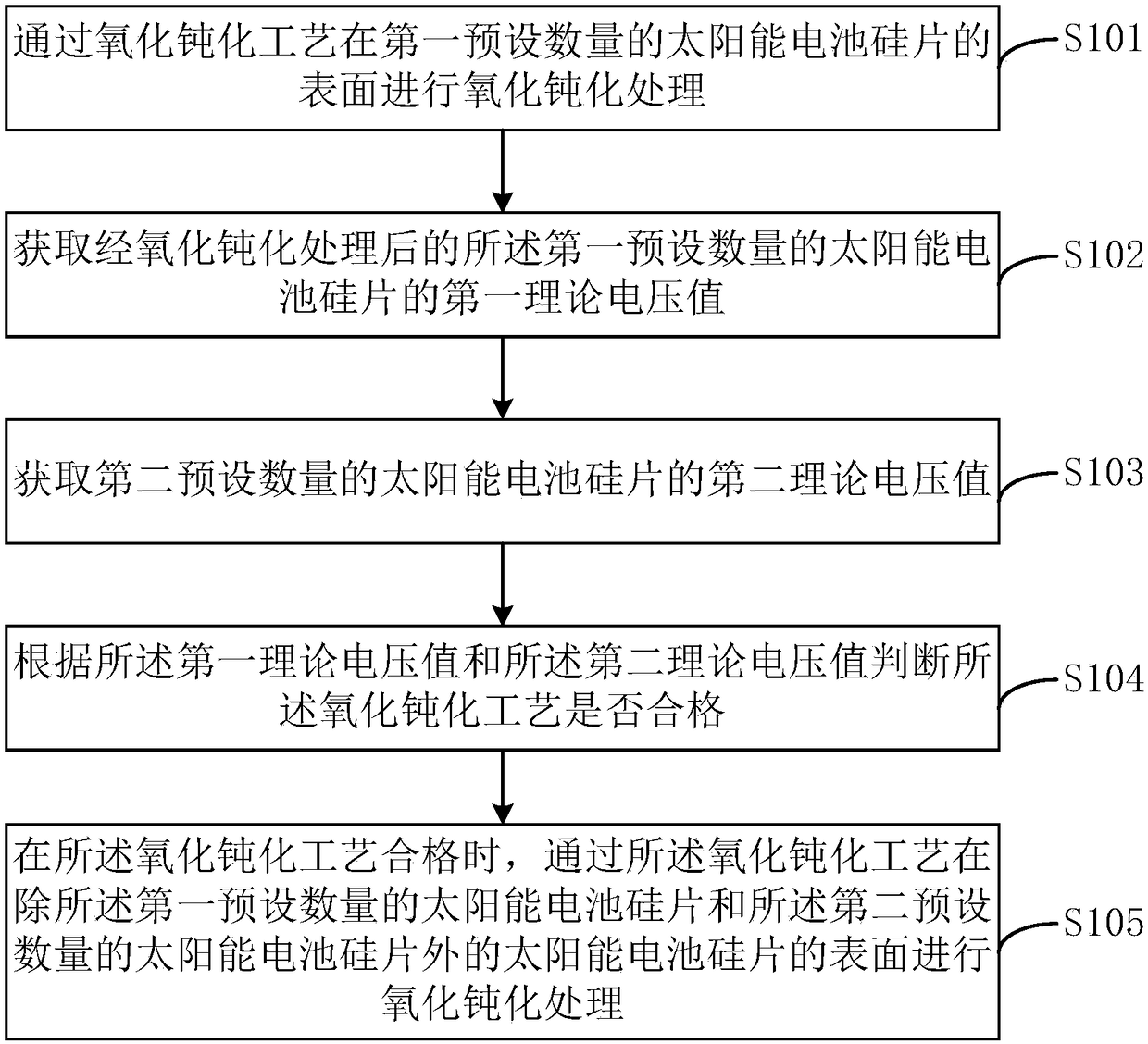
[0045] Please refer to figure 1 , the oxidation passivation method of solar cell silicon wafer comprises the steps:
[0046] Step S101 , performing oxidation passivation treatment on the surface of a first preset number of silicon wafers of solar cells through an oxidation passivation process.
[0047] In the embodiment of the present invention, the silicon wafers used to produce solar cells are subjected to the process steps of texturing and polishing the back field, preparation of the front emitter, back etching, ion implantation, cleaning and annealing, and before the oxidation passivation process, A first preset number of solar cell silicon wafers and a second preset number of solar cell silicon wafers are respectively selected among the solar cell silicon wafers. In an implementation manner, a first pre...
Embodiment 2
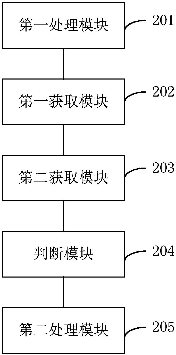
[0068] Please refer to figure 2 , Embodiment 2 of the present invention provides an oxidation passivation device for silicon wafers of solar cells, comprising:
[0069] The first processing module 201 is used to perform oxidation passivation treatment on the surface of a first preset number of solar cell silicon wafers through an oxidation passivation process;
[0070] A first acquisition module 202, configured to acquire a first theoretical voltage value of the first preset number of silicon wafers of solar cells after oxidation passivation treatment;
[0071] The second acquisition module 203 is configured to acquire a second theoretical voltage value of a second preset number of silicon wafers of solar cells;
[0072] A judging module 204, configured to judge whether the oxidation passivation process is qualified according to the first theoretical voltage value and the second theoretical voltage value;
[0073] The second processing module 205 is configured to remove the...
Embodiment 3
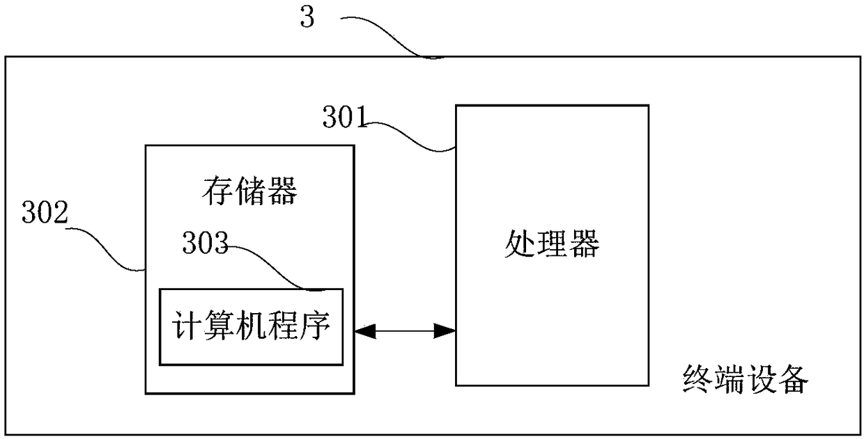
[0088] image 3 It is a schematic diagram of oxidation passivation terminal equipment for silicon wafers of solar cells provided by an embodiment of the present invention. Such as image 3As shown, the terminal device 3 for oxidation passivation of solar cell silicon wafers in this embodiment includes: a processor 301 , a memory 302 , and a computer program 303 stored in the memory 302 and operable on the processor 301 . When the processor 301 executes the computer program 303, it realizes the steps in the above embodiments of the oxidation passivation method for silicon wafers of solar cells, for example figure 1 Steps S101 to S105 are shown. Alternatively, when the processor 301 executes the computer program 303, it realizes the functions of the modules / units in the above-mentioned device embodiments, for example figure 2 The functions of modules 201 to 205 are shown.
[0089] Exemplarily, the computer program 303 may be divided into one or more modules / units, and the o...
PUM
 Abstract
Description
Claims
Application Information
 - Generate Ideas
- Intellectual Property
- Life Sciences
- Materials
- Tech Scout
- Unparalleled Data Quality
- Higher Quality Content
- 60% Fewer Hallucinations
Browse by: Latest US Patents, China's latest patents, Technical Efficacy Thesaurus, Application Domain, Technology Topic, Popular Technical Reports.
© 2025 PatSnap. All rights reserved.Legal|Privacy policy|Modern Slavery Act Transparency Statement|Sitemap|About US| Contact US: help@patsnap.com


