
Low-noise and high-ground-up-noise-resistant output driving circuit and method

A technology for outputting drive circuits and ground bounce noise, which is applied in logic circuits, logic circuit coupling/interface using field effect transistors, logic circuit connection/interface layout, etc. Ground bounce noise, large static power consumption, etc., to achieve the effect of reducing ground bounce noise, improving the ability to resist high ground bounce noise, and reducing the current rate of change

Pending Publication Date: 2018-09-04
AMICRO SEMICON CORP
View PDF1 Cites 6 Cited by
  • Summary
  • Abstract
  • Description
  • Claims
  • Application Information

AI Technical Summary

Problems solved by technology

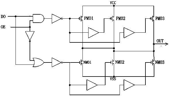
However, this circuit still has relatively large disadvantages: first, the IO drive circuit has PMOS transistors PMO1, PMOS transistors PMO2 and PMOS transistors PMO3 that are turned on almost simultaneously, or NMOS transistors NMO1, NMOS transistors NMO2 and NMOS transistors NMO3 are turned on almost simultaneously. It causes a large current to charge the load capacitor through the PMOS tube or discharge the load capacitor through the NMOS tube in a short period of time, resulting in a large ground bounce noise; secondly, in the static working state of the circuit, the PMOS tube or NMOS tube is always turned on , which will introduce ground bounce noise and will also generate large static power consumption
[0005] In addition, some IO drive circuit design technologies that intentionally reduce ground bounce noise in the prior art, such as US Patent No. 4880997, control the drive capability of the pre-driver to make the final stage drive PMOS transistor and NMOS transistor slowly turned on, but they are still not effective. Eliminate the error phenomenon of the output signal level caused by the ground bounce signal generated by multiple IO drive circuits working at the same time

Method used


Image

  • Low-noise and high-ground-up-noise-resistant output driving circuit and method
  • Low-noise and high-ground-up-noise-resistant output driving circuit and method
  • Low-noise and high-ground-up-noise-resistant output driving circuit and method

Examples


Embodiment approach

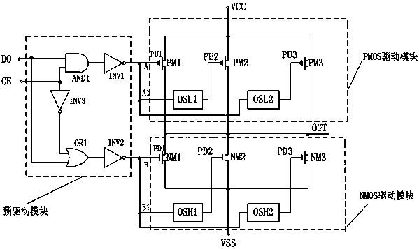
[0043] As an embodiment of the present invention, the PMOS drive module includes a preset number of falling edge delay control sub-modules and PMOS tubes divided into preset groups, and the settings of the preset number of groups and each group The setting of the number of PMOS transistors all meets the actual drive capability of the chip IO, wherein the preset number is equal to the preset number of groups minus one; each group of PMOS transistors in the remaining groups except the first group of PMOS transistors The PMOS transistor corresponds to a falling edge delay control sub-module; in the embodiment of the present invention, in order to simplify the description, the preset number of groups is set to 3, the preset number is set to 2, and all the PMOS transistors in each group are connected in parallel. can be simplified to an equivalent PMOS transistor, such as figure 2 As shown, the first group of PMOS transistors is simplified as the first PMOS transistor PM1, the sec...


PUM


Abstract

The invention discloses a low-noise and high-ground-up-noise-resistant output driving circuit and method. The circuit is divided into a pre-driving module, a PMOS driving module and an NMOS driving module, the PMOS driving module and the pre-driving module are connected to a PMOS input node, and the NMOS driving module and the pre-driving module are connected to an NMOS input node, so that outputdriving resistance of the output driving circuit is dynamically adjusted so as to reduce the ground-up noise when a dynamic signal is input at the PMOS input node or the NMOS input node; and the output driving resistance is improved to enhance the high ground-up noise resistant effect when a static signal is input at the PMOS input node or the NMOS input node. Compared with the prior art, the output driving resistance of the output driving circuit is dynamically adjusted, so as to reduce the ground-up noise; meanwhile, the output resistance is improved when in static driving, so as to improvethe high ground-up noise effect resistance.

Description

technical field [0001] The invention relates to a semiconductor integrated circuit, in particular to an output driving circuit with low noise and anti-high ground bounce noise and a method for reducing ground bounce noise based on the output driving circuit. Background technique [0002] There is a package inductance between the power supply on the circuit board and the packaged case power supply, there is an on-chip parasitic inductance between the packaged case power supply and the internal power supply of the semiconductor integrated circuit, and there is a packaged inductance between the ground wire on the circuit board and the packaged case ground wire , There is an on-chip parasitic inductance between the package shell wire ground and the internal ground wire of the semiconductor integrated circuit. Generally speaking, the package inductance is much larger than the on-chip parasitic inductance, and there is a large transient current change in the power line and ground ...

Claims


Application Information

Patent Timeline
Patent Type & Authority Applications(China)
IPC IPC(8): H03K19/0185H03K19/003
CPCH03K19/00315H03K19/018507
Inventor 杨秋平
Owner AMICRO SEMICON CORP
Learn More