Automatic correction circuit and correction method of amplifier input offset voltage

A technology of amplifier circuit and offset voltage, which is applied in the direction of improving amplifiers to reduce temperature/power supply voltage changes, amplifiers, differential amplifiers, etc., and can solve the problems of fully differential output voltage errors, single-ended output voltage vout errors, and deviations.

Pending Publication Date: 2018-09-04
AMICRO SEMICON CORP
View PDF0 Cites 13 Cited by
  • Summary
  • Abstract
  • Description
  • Claims
  • Application Information

AI Technical Summary

Problems solved by technology

Since the fully differential amplifier offset voltage exists, resulting in a fully differential output voltage of the amplified output with differential input voltage Expected magnification value of There is a deviation, especially when the amplitude of the differential input signal vip-vin is originally small, due to the existence of the offset of the op amp, the offset feedback voltage value relative to The value of is not negligible. Obviously, there will be a large error for the fully differential output voltage. If it is not correct for the offset feedback voltage caused by the offset of the op amp corrected, then the fully differential output voltage The value of the differential input voltage with the expected value of big difference
[0004] figure 2 It is a circuit schematic diagram of a typical application of a single-ended operational amplifier. The negative input terminal of the differential amplifier inputs the voltage vin through a negative input resistor with a resistance value of R1, and the positive input terminal of the differential amplifier inputs a reference voltage vref through a positive input resistor with a resistance value of R1. The output terminal of the differential amplifier is connected back to the negative input terminal of the differential amplifier through a negative feedback resistor with a resistance value of R2, and the single-ended output voltage of the differential amplifier is , due to the offset voltage of the single-ended amplifier exists, resulting in the desired amplified value of the single-ended output voltage vout and the differential input voltage There is a deviation, especially when the difference between the single-ended output voltage vout and the reference voltage vref is not large, due to the existence of the operational amplifier offset value greater than Obviously, there will be a large error for the single-ended output voltage vout. At this time, if the offset feedback voltage caused by the offset of the op amp is not correct Correction, then the single-ended output voltage vout value and the expected amplification value of the differential input voltage Significant difference

Method used


Image

  • Automatic correction circuit and correction method of amplifier input offset voltage
  • Automatic correction circuit and correction method of amplifier input offset voltage
  • Automatic correction circuit and correction method of amplifier input offset voltage

Examples


Embodiment Construction

[0064] The specific embodiment of the present invention will be further described below in conjunction with accompanying drawing:

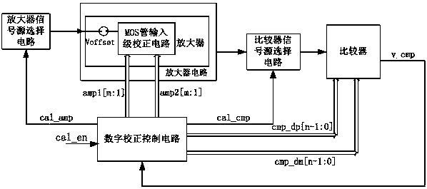
[0065] Such as image 3 As shown, an automatic correction circuit for amplifier input offset voltage includes an amplifier signal source selection circuit, an amplifier circuit, a comparator signal source selection circuit, a comparator and a digital correction control circuit.

[0066] The digital correction control circuit includes a comparator enabling terminal cal_cmp connected to the comparator signal source selection circuit, a first auxiliary correction control encoding signal terminal amp1 and a second auxiliary correction control encoding signal terminal amp2. The logic of controlling the offset voltage correction of the comparator in the digital correction control circuit is: when the comparator offset correction enable terminal cal_cmp is at a high level, the digital correction control circuit adjusts the first auxiliary correction cont...


PUM


Abstract

The invention discloses an automatic correction circuit of amplifier input offset voltage, and a correction method thereof. The automatic correction circuit firstly accomplishes the auxiliary correction through comparator own offset voltage, and then adjusts the width-to-length ratio of a MOS tube in a MOS tube input-level correction circuit in the amplifier, thereby realizing the correction of the input offset voltage of the whole amplifier; compared with the prior art, the differential input level of the amplifier is modified so that the equivalent width-to-length ratio of the input differential MOS tube pair can be controlled by a digital control code value, the input-level offset voltage of the amplifier is not corrected by compensating the output voltage value of the amplifier, and the correction of the full-differential amplifier offset voltage can be accomplished without continuously adjusting the analog voltage; the acquired corresponding digital control code value can be reserved when the correction is finished, thereby improving the working precision of the subsequent amplifier; and the auxiliary correction of the digital correction control circuit is stopped, so that thepower consumption is saved.

Description

technical field [0001] The invention relates to the field of analog circuit design, in particular to an automatic correction circuit and correction method for amplifier input offset voltage. Background technique [0002] The operational amplifier is a basic analog circuit function module, which is widely used. The DC offset voltage in the operational amplifier has also been widely concerned by the industry. Major companies have also proposed corresponding solutions that use analog control methods to control the DC offset voltage. For correction, their design is mainly to correct the input offset voltage of the amplifier by compensating the output voltage value of the amplifier. However, the input stage of the entire operational amplifier may still introduce an offset voltage. [0003] In some op amp applications, for example, figure 1 It is a schematic circuit diagram of a typical application of a fully differential operational amplifier, in which the positive input termina...

Claims


Application Information

Patent Timeline
Patent Type & Authority Applications(China)
IPC IPC(8): H03F1/30H03F3/45
CPCH03F1/301H03F3/45206H03F2203/45134
Inventor 杨秋平
Owner AMICRO SEMICON CORP
Why Eureka
Try Eureka