Manufacturing method for stepped groove with non-metallic side walls and PCB
A production method and non-metallization technology, which is applied to printed circuits connected with non-printed electrical components, multi-layer circuit manufacturing, printed circuit manufacturing, etc., can solve the problems of complex manufacturing process, poor versatility, and difficult operation, and achieve Simplify the production process, improve work efficiency, and reduce the difficulty of operation
- Summary
- Abstract
- Description
- Claims
- Application Information
AI Technical Summary
Problems solved by technology
Method used
Image
Examples
Embodiment 1
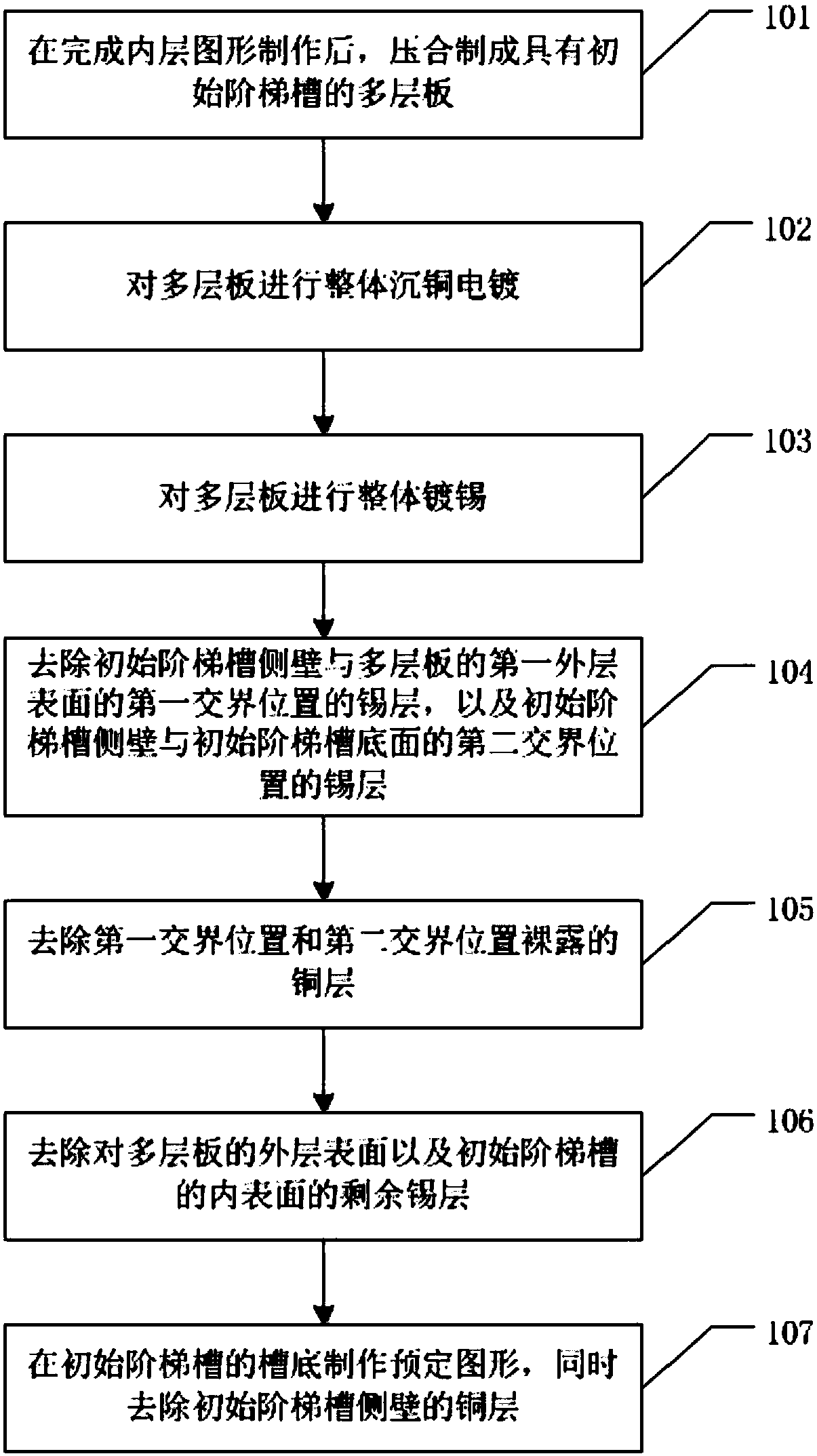
[0059] see figure 1 , the first embodiment provides a method for fabricating a stepped groove with a non-metallized sidewall, including the steps:
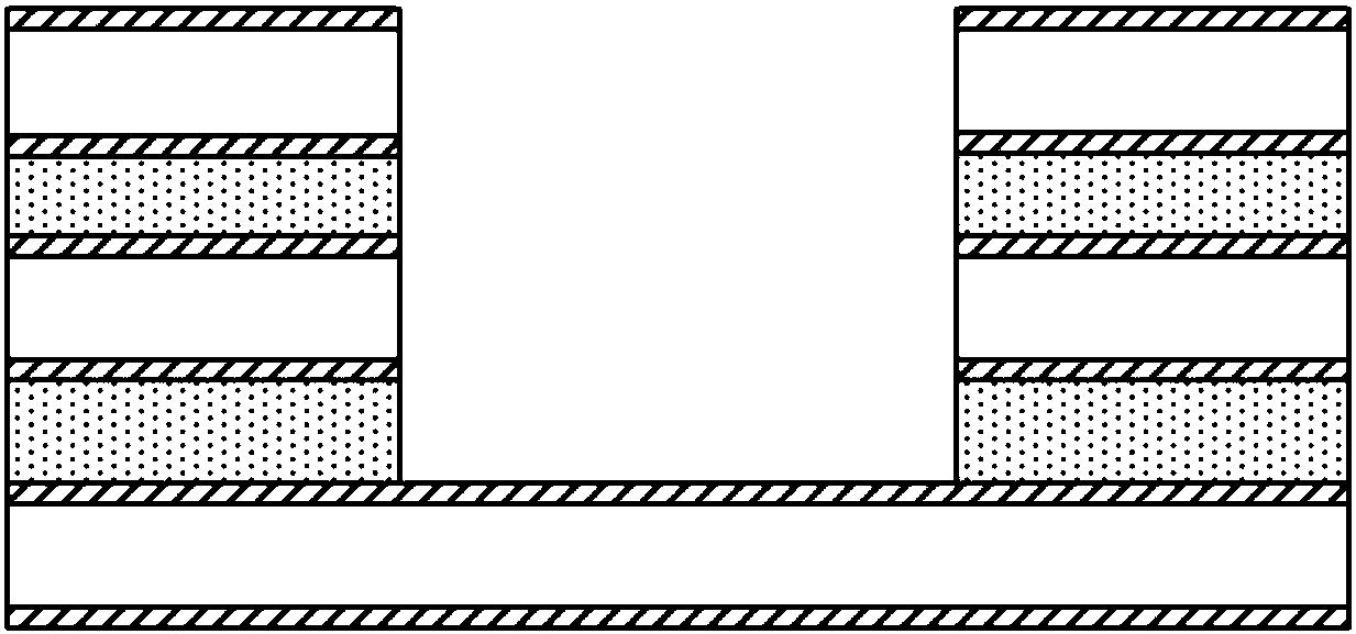
[0060] Step 101. After the inner layer pattern is completed, a multi-layer board with an initial stepped groove is formed by pressing, such as figure 2 shown.
[0061] Wherein, the multi-layer board includes a first outer layer surface and a second outer layer surface distributed along the stacking direction, and the bottom surface and sidewall of the initial stepped groove are not metallized; the initial stepped groove can be filled or embedded with gaskets. To make the molding, the notch of the initial stepped groove is formed on the surface of the first outer layer.
[0062] The method of making the initial stepped groove by using the embedded gasket method is as follows: complete the inner layer graphics of each core board respectively; open windows at the preset positions on the specified inner core board and the specified...
Embodiment 2
[0082] The second embodiment provides another method for fabricating a stepped groove with a non-metallized sidewall. The groove bottom of the stepped groove is not only formed with a predetermined pattern but also has a via hole.
[0083] see Figure 12 As shown, the manufacturing method of the stepped groove in this embodiment includes the steps:
[0084] Step 201 , forming an initial stepped groove, and neither the bottom surface nor the side wall of the initial stepped groove is metallized.
[0085] Step 202: Open via holes inside and outside the initial stepped groove, and perform overall copper immersion plating on the multilayer board, so that the outer surface of the multilayer board (including the first outer layer surface and the second outer layer surface distributed along the stacking direction), the initial The inner surface of the stepped groove (including the sidewall and bottom surface of the initial stepped groove) and the inner wall of the via hole are plate...
Embodiment 3
[0099] The third embodiment provides a PCB, which includes a stepped groove with a non-metallized sidewall, and the stepped groove is manufactured according to the manufacturing method provided in the first embodiment or the second embodiment.
PUM
 Abstract
Description
Claims
Application Information
 - R&D
- Intellectual Property
- Life Sciences
- Materials
- Tech Scout
- Unparalleled Data Quality
- Higher Quality Content
- 60% Fewer Hallucinations
Browse by: Latest US Patents, China's latest patents, Technical Efficacy Thesaurus, Application Domain, Technology Topic, Popular Technical Reports.
© 2025 PatSnap. All rights reserved.Legal|Privacy policy|Modern Slavery Act Transparency Statement|Sitemap|About US| Contact US: help@patsnap.com


