
Flash memory and manufacturing method thereof

A manufacturing method and flash memory technology, applied in the manufacture of flash memory and the field of flash memory, can solve the problems of reducing the distance of flash memory cells and affecting the performance of flash memory cells, and achieve the effect of simple process

Active Publication Date: 2018-07-27
SHANGHAI HUALI MICROELECTRONICS CORP
View PDF4 Cites 4 Cited by
  • Summary
  • Abstract
  • Description
  • Claims
  • Application Information

AI Technical Summary

Problems solved by technology

However, this structure will reduce the distance between adjacent flash memory cells, resulting in mutual interference between flash memory cells (Disturb), and this problem will continue to worsen with the reduction of the N+ diffusion area, thereby affecting the performance of flash memory cells

Method used


Image

  • Flash memory and manufacturing method thereof
  • Flash memory and manufacturing method thereof
  • Flash memory and manufacturing method thereof

Examples


Embodiment Construction

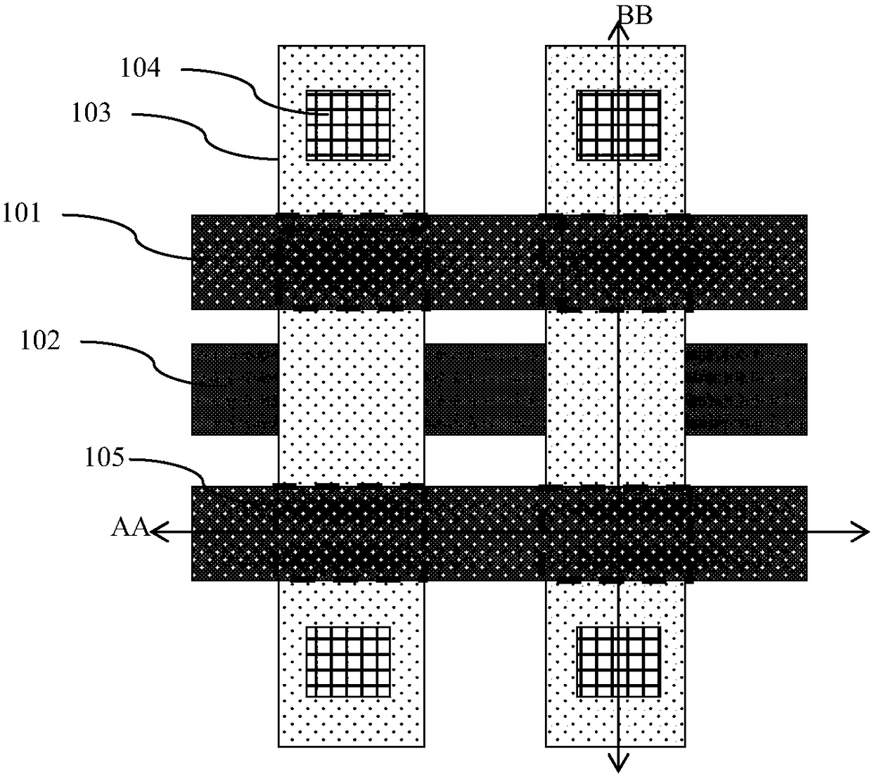
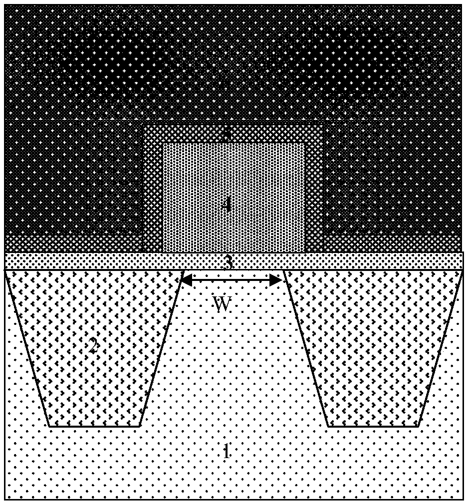
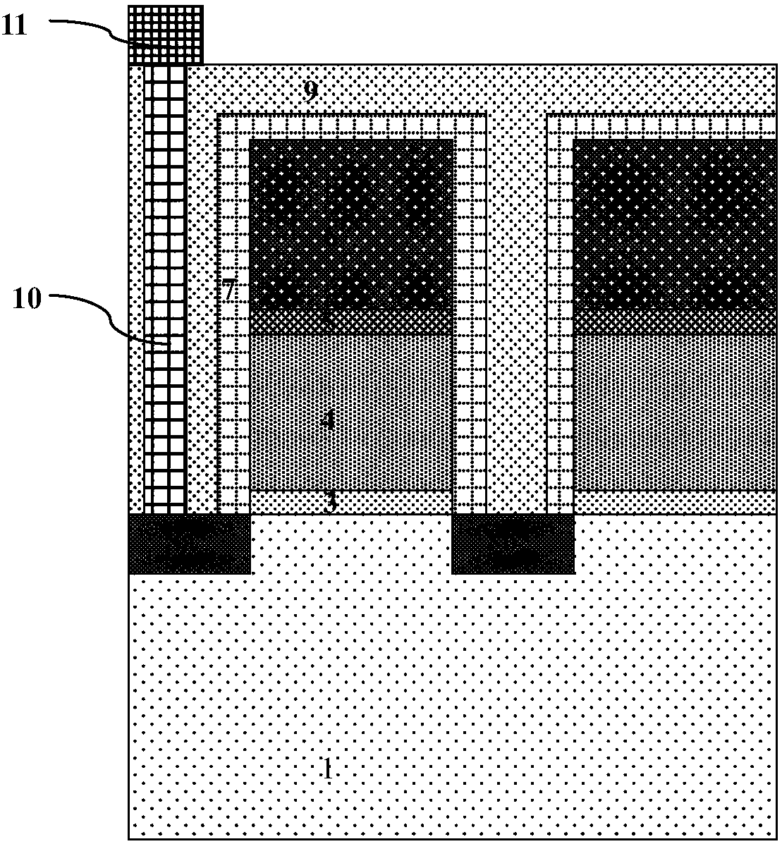
[0069] Please also refer to the layout structure of the flash memory of the embodiment of the present invention Figure 4 as shown, Figure 8 is the edge of the flash memory of the embodiment of the present invention Figure 4 Sectional view of CC line; Figure 9 is the edge of the flash memory of the embodiment of the present invention Figure 4 Sectional view of line DD in middle; Figure 4 It can be known from the layout structure that the storage area of ​​the flash memory in the embodiment of the present invention includes a flash memory cell array formed by arranging a plurality of flash memory cells. Each flash memory cell of the flash memory cell array is formed in the same active area 201 . The top of the polysilicon row 202 formed by the polysilicon control gate 407 is connected to the word line formed by the front metal layer; the polysilicon floating gate 403 is connected to the Figure 4 The formation area in is shown in the dotted line box 203, the N+ diffus...


PUM


Abstract

The invention discloses a flash memory. Each flash memory is formed in the same active region, poly-silicon control gates at the same line are connected to form a poly-silicon line, N+ diffusion regions are symmetrically formed at two sides of each poly-silicon floating gate, each N+ diffusion region at the same row is connected to form an N+ diffusion region row, channel regions are arranged among the N+ diffusion region rows and are covered by the poly-silicon floating gates, each poly-silicon floating gate is formed by laminating a bottom poly-silicon floating gate and a top poly-silicon floating gate, the length of the top poly-silicon floating gate is smaller than the length of the bottom of the bottom poly-silicon floating gate, the length of the channel region is defined by the bottom poly-silicon floating gate in an alignment way, a third dielectric layer covers a surface of each N+ diffusion region, and a surface of the third dielectric layer is lower than or equal to a surface of the bottom poly-silicon floating gate. The invention also discloses a manufacturing method of the flash memory. By the flash memory, the coupling rate between the poly-silicon control gate and the poly-silicon floating gate can be improved, and meanwhile, the mutual interference between adjacent poly-silicon floating gates can be reduced.

Description

technical field [0001] The invention relates to the field of semiconductor integrated circuits, in particular to a flash memory (Flash), and also to a method for manufacturing the flash memory. Background technique [0002] Flash memory has been widely used as the best choice for non-volatile memory applications due to its advantages of high density, low price, and electrical programmability and erasability. At present, flash memory cells are mainly implemented at the 65nm technology node. With the demand for large-capacity flash memory, the number of chips on each silicon wafer will be reduced by using the existing technology nodes. At the same time, the increasing maturity of new technology nodes also urges flash memory cells to be produced with high-node technology, which means that the size of flash memory cells needs to be reduced. [0003] The first type of flash memory unit is available: [0004] Now the first common structure of flash memory cells has a contact hol...

Claims


Application Information

Patent Timeline
IPC IPC(8): H01L27/11524
CPCH10B41/35
Inventor 田志钟林建
Owner SHANGHAI HUALI MICROELECTRONICS CORP
Learn More