Crystalline silicon cell with high resistance to mechanical load
A crystalline silicon cell and mechanical load technology, applied in the field of solar cells, can solve the problems of increased material cost, cumbersome process steps, increased labor cost, etc., and achieve the effect of reducing fragmentation rate, simple process and good compatibility
- Summary
- Abstract
- Description
- Claims
- Application Information
AI Technical Summary
Problems solved by technology
Method used
Image

Examples
Embodiment 1
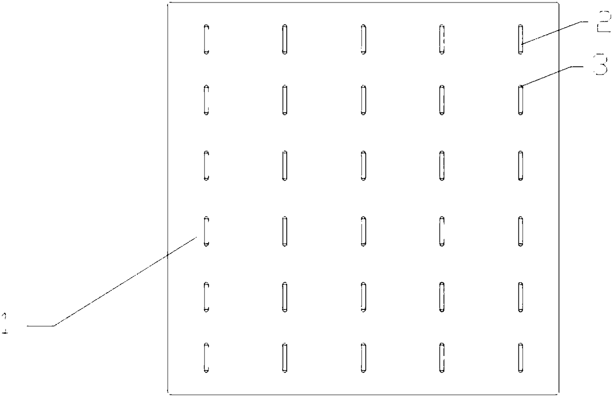
[0041] Such as figure 1 As shown, in the crystalline silicon battery with high mechanical load resistance provided by this embodiment, the back electrode of the crystalline silicon battery includes multiple columns of grid lines 1 distributed in parallel, and each column of grid lines includes six sections of sub-grid lines 2 arranged at intervals. A gap 3 is provided between the two ends of each sub-grid line and the back electric field.
[0042] Among them, the crystalline silicon battery adopts p-type polycrystalline silicon wafer.
[0043] The preparation method of the crystalline silicon battery with high mechanical load resistance comprises the following steps:
[0044] (1) Select a lightly doped p-type polysilicon wafer with a resistivity of 0.1-6Ω·cm, place the silicon wafer substrate in a texturing machine to remove the damaged layer and prepare the textured surface. The chemical solution used for texturing is hydrogen fluoride One or more mixed aqueous solutions of...
Embodiment 2
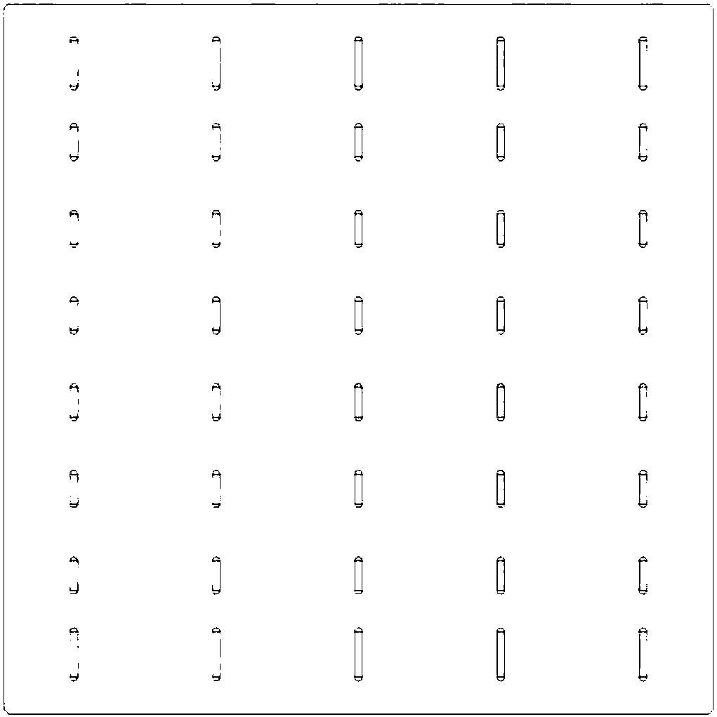
[0055]As shown in the figure, the difference from Embodiment 1 is that a p-type polysilicon wafer is used, and the back electrode includes multiple columns of gate lines arranged in parallel, and each gate line is composed of eight sub-gate lines arranged at intervals.
[0056] As shown in Table 2, according to the above examples, the results show that the debris rate at the end of the polycrystalline silicon battery module has decreased by more than 0.2%.
[0057] Table 2 Performance comparison between polycrystalline silicon battery components prepared in this example and conventional battery components
[0058] battery pack
Embodiment 3
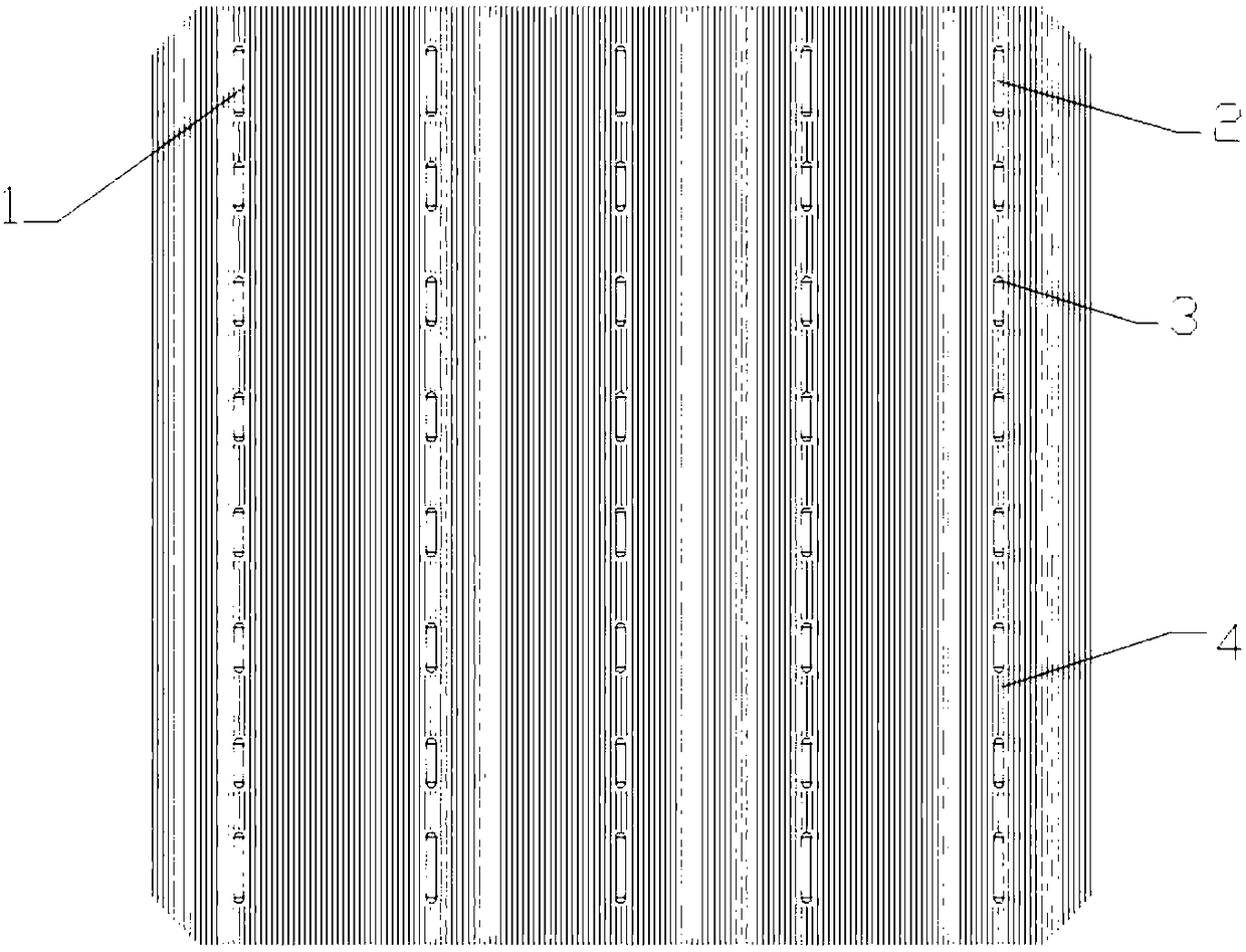
[0060] Such as image 3 As shown, in the crystalline silicon cell with high mechanical load resistance provided in this embodiment, the back electrode of the crystalline silicon cell includes multiple columns of grid lines 1 distributed in parallel, and each column of grid lines includes eight sub-gate lines 2 arranged at intervals. A gap 3 is provided between the two ends of each sub-grid line and the back electric field.
[0061] The crystalline silicon wafer is a p-type PERC single crystal silicon wafer.
[0062] A passivation film is provided on the back of the PERC crystalline silicon cell, and a laser slotting line 4 is provided on the passivation film, and the laser slotting line 4 is disconnected at the position of the back electrode.
[0063] The passivation film is preferably an aluminum oxide and silicon nitride laminated passivation film.
[0064] The preparation method of the crystalline silicon battery with high mechanical load resistance comprises the followin...
PUM
 Abstract
Description
Claims
Application Information
 - R&D
- Intellectual Property
- Life Sciences
- Materials
- Tech Scout
- Unparalleled Data Quality
- Higher Quality Content
- 60% Fewer Hallucinations
Browse by: Latest US Patents, China's latest patents, Technical Efficacy Thesaurus, Application Domain, Technology Topic, Popular Technical Reports.
© 2025 PatSnap. All rights reserved.Legal|Privacy policy|Modern Slavery Act Transparency Statement|Sitemap|About US| Contact US: help@patsnap.com