Eureka AIR delivers breakthrough ideas for toughest innovation challenges, trusted by R&D personnel around the world.

PCB of preventing separating of hole walls, and processing technology thereof

A technology of PCB board and processing technology, which is applied in the field of PCB board, can solve problems such as hidden dangers buried downstream of PCB, high claims made by electronic manufacturers, and economic loss of PCB, so as to avoid hole wall separation, increase connection force, and increase bonding force Effect

Pending Publication Date: 2018-05-08
广州广合科技股份有限公司
View PDF0 Cites 2 Cited by
  • Summary
  • Abstract
  • Description
  • Claims
  • Application Information

AI Technical Summary

Problems solved by technology

[0002] Hole wall separation is a defect in which the copper plating layer of the plated through hole is separated from the PCB body during the heat treatment of PCB and PCBA (hot air leveling tin, thermal shock, reflow soldering), etc. Once it occurs, it will bury the PCB downstream. Hidden danger
Once a PCB manufacturer or its downstream customers discover the phenomenon of hole wall separation, they will always scrap or return the whole batch, which will directly cause huge economic losses to the PCB manufacturer. What's more, it is often accompanied by High claims of electronic manufacturers

Method used


Image

  • PCB of preventing separating of hole walls, and processing technology thereof
  • PCB of preventing separating of hole walls, and processing technology thereof
  • PCB of preventing separating of hole walls, and processing technology thereof

Examples


Embodiment Construction

[0027] In order to facilitate the understanding of those skilled in the art, the present invention will be further described in detail below in conjunction with the accompanying drawings and embodiments:

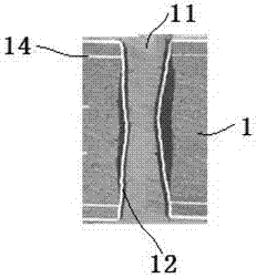
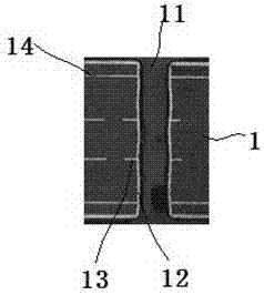
[0028] Such as figure 1 , a kind of PCB board that prevents hole wall separation, is characterized in that, comprises PCB board body 1, and described PCB board body 1 is provided with several mutually parallel conductive copper layers 14 and PTH hole 11, and described PTH hole 11 is perpendicular to described The conductive copper layer 14 is provided, and the hole wall of the PTH hole 11 is provided with a copper-plated layer 12, and the outer side of the copper-plated layer 12 is fixedly provided with several annular rings 13, and the annular ring 13 surrounds the copper-plated layer 12 set, and the annular ring 13 is embedded in the PCB board body 1 .

[0029] In one embodiment, the center of the annular ring 13 is located on the centerline of the PTH hole 11 .

[0030]...


PUM


Abstract

The invention relates to a PCB of preventing separating of hole walls. The PCB of preventing separating of hole walls is characterized in that the PCB of preventing separating of hole walls includes aPCB body; a plurality of mutually parallel conductive copper layers and PTH holes are formed in the PCB body 1; the PTH holes are perpendicular to the conductive copper layers; copper plates are arranged on the hole walls of the PTH holes; a plurality of hole rings are fixedly at the outer side of each copper plate, and the hole rings encircle the copper plate; and the hole rings are embedded into the PCB body. The PCB of preventing separating of hole walls can effectively avoid the copper plates separating from hole walls of the PTH holes by increasing the hole rings.

Description

technical field [0001] The invention relates to the field of circuit boards, in particular to a PCB board for preventing hole wall separation. Background technique [0002] Hole wall separation is a defect in which the copper plating layer of the plated through hole is separated from the PCB body during the heat treatment of PCB and PCBA (hot air leveling tin, thermal shock, reflow soldering), etc. Once it occurs, it will bury the PCB downstream. Hidden danger. Once a PCB manufacturer or its downstream customers find that the hole wall is separated, they will always scrap or return the whole batch, which will directly cause huge economic losses to the PCB manufacturer. What is more serious is that it is often accompanied by High claims for electronics manufacturers. Now that the thickness of PCB is getting thicker and thicker, the probability of hole wall separation also increases accordingly. Contents of the invention [0003] Based on this, it is necessary to provide ...

Claims


Application Information

Patent Timeline
IPC IPC(8): H05K1/11H05K3/42
CPCH05K1/115H05K3/42H05K2203/1105
Inventor 向参军彭镜辉
Owner 广州广合科技股份有限公司
Why Eureka
Eureka Blog
Learn More