led light and led packaging process

A technology of LED packaging and packaging technology, applied in semiconductor devices, electrical components, circuits, etc., can solve the problems of quantum efficiency decline, light intensity reduction, spectral shift, etc., and achieve the effect of improving luminous dispersion

Active Publication Date: 2019-11-15
广东安林电子科技股份有限公司
View PDF8 Cites 0 Cited by
  • Summary
  • Abstract
  • Description
  • Claims
  • Application Information

AI Technical Summary

Problems solved by technology

[0004] LEDs that use the above method to emit light have the following defects: the distribution of light emitted by the LED light source is relatively scattered, and the illumination brightness of the light source is not good. It often needs to be shaped by an external lens to meet the brightness requirements, which greatly increases the production cost of the LED; The powder is directly coated on the surface of the chip, and the chip absorbs the scattered light, which reduces the luminous efficiency. Moreover, the high temperature of the chip will reduce the quantum efficiency of the phosphor powder, which will affect the lumen efficiency of the LED light source, which will easily lead to a decrease in light intensity. A series of problems such as spectral shift and accelerated aging of the chip reduce the service life of the LED light source

Method used


Image

  • led light and led packaging process
  • led light and led packaging process
  • led light and led packaging process

Examples


Embodiment 1

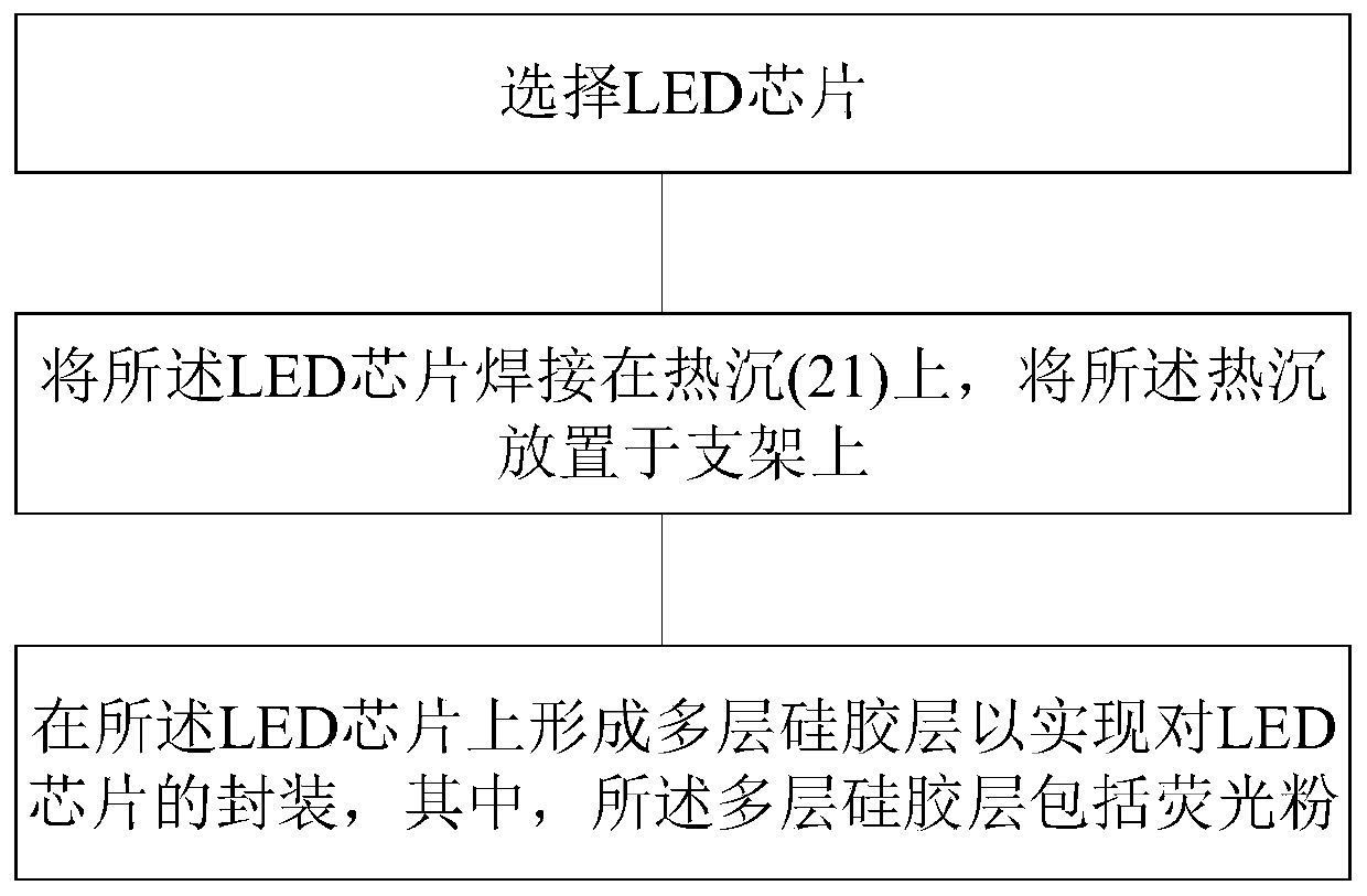
[0051] See figure 1 , figure 1 A schematic diagram of an LED packaging process flow provided by an embodiment of the present invention, the method includes:

[0052] Select the LED chip;

[0053] Welding the LED chip on the heat sink (21), placing the heat sink (21) on the bracket;

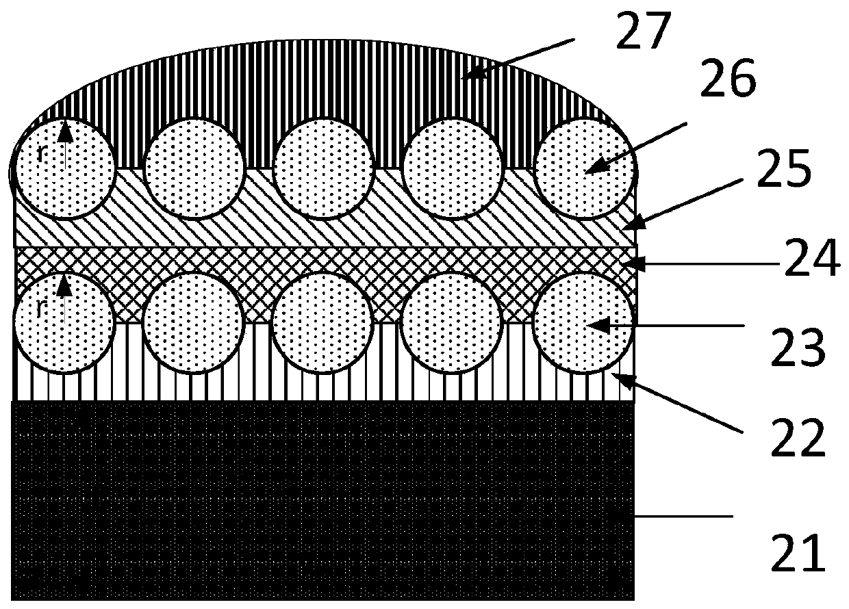
[0054] A multi-layer silicone layer is formed on the LED chip to realize the packaging of the LED chip, wherein the silicone layer in contact with the LED chip in the multi-layer silicone layer does not contain fluorescent powder.

[0055]In this embodiment, the silica gel layer in direct contact with the LED chip does not contain phosphor, and the phosphor is placed in other silica gel layers that do not directly contact the LED chip, avoiding direct contact between the phosphor powder and the LED chip. The reason for the implementation is: the chip has an absorption effect on the backscattered light, and the implementation of phosphor powder directly coated on the LED chip will reduce the lig...

Embodiment 2

[0093] This embodiment further illustrates the packaging method of the LED chip provided by the present invention.

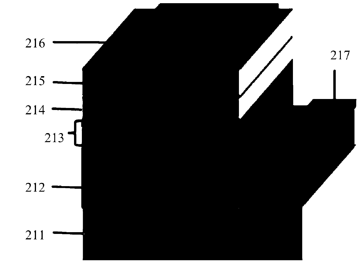
[0094] see again Figure 6 ,exist Figure 6In the shown heat sink, the width W of the heat sink is 0.5 mm to 10 mm, the diameter R of the circular through hole is 0.2 mm to 1 mm, and the distance L2 between two connected circular through holes is 0.5 mm to 10 mm. The thickness D and length L of the sink, and the distance L1 between the initial circular through hole and the heat sink wall can be determined according to the process conditions, and the present invention is not limited here.

[0095] Preferably, the thickness of the heat sink used in this embodiment is relatively thick, so the heat sink will not affect the heat dissipation effect due to the reduction of the degree of fit between the heat sink and the peripheral heat dissipation device due to high temperature deformation.

[0096] In this embodiment, the first silica gel layer (22) is arranged on t...


PUM


Abstract

The invention relates to an LED lamp and an LED packaging technology. The packaging technology comprises the steps of selecting an LED chip; welding the LED on heat sink (21) and arranging the heat sink (21) on a bracket; and forming multiple silica gel layers on the LED chip to achieve packaging of the LED chip, wherein the silica gel layer, in contact with the LED chip, in the multiple silica gel layers does not contain fluorescent powder. According to the LED packaging technology, the fluorescent powder is separated from the LED chip, so that the problem that the quantum efficiency of the fluorescent powder is reduced due to high temperature is solved; and silica gel in contact with the LED chip is high-temperature resistant silica gel, so that the problem that the light transmittance is reduced due to ageing and yellowing of the silica gel is solved.

Description

technical field [0001] The invention belongs to the technical field of semiconductors, and in particular relates to an LED lamp and an LED packaging process. Background technique [0002] LED (Light Emitting Diode), light-emitting diode, is a solid-state semiconductor device that can directly convert electricity into light. The practicality and commercialization of high-performance LEDs have brought about a new revolution in lighting technology. The pixel light composed of multiple ultra-high-brightness red, blue, and green LEDs can not only emit various colors of light with continuously adjustable wavelengths, but also emit white light with a brightness of tens to one hundred candlepower as a lighting source. For incandescent lamps and LED solid-state lighting lamps with the same luminance, the power consumption of the latter only accounts for 10%-20% of the former. [0003] Most of the white LEDs currently produced are made by covering a layer of light yellow phosphor co...

Claims


Application Information

Patent Timeline
Patent Type & Authority Patents(China)
IPC IPC(8): H01L33/62H01L33/64H01L33/50
CPCH01L33/502H01L33/62H01L33/64
Inventor 左瑜
Owner 广东安林电子科技股份有限公司
Why Eureka
Try Eureka