LED package method

A technology of LED packaging and LED chips, applied in semiconductor devices, electrical components, circuits, etc., can solve the problems of irradiating light, reducing the quantum efficiency of phosphor powder, and inconcentrating light, and achieve the effect of avoiding total reflection.

Active Publication Date: 2018-05-08
YANGZHOU HUACAI OPTO ELECTRONICS
View PDF3 Cites 0 Cited by
  • Summary
  • Abstract
  • Description
  • Claims
  • Application Information

AI Technical Summary

Problems solved by technology

[0004] 1. Since the light emitted by the LED light source is generally distributed in a divergent manner, the light is not concentrated, and the secondary shaping through the external lens increases the production cost;
[0005] 2. Phosphor powder is generally directly coated on the surface of the chip. The high temperature generated by the LED chip reduces the quantum efficiency of the phosphor powder. In addition, the chip absorbs the light reflected back by the phosphor powder, which reduces the light extraction of the packaging structure. efficiency;
[0006] 3. Due to the blocking effect of the packaging structure on light, the light cannot be fully irradiated from the packaging structure, and the light transmittance is low

Method used


Image

  • LED package method
  • LED package method
  • LED package method

Examples


Embodiment 1

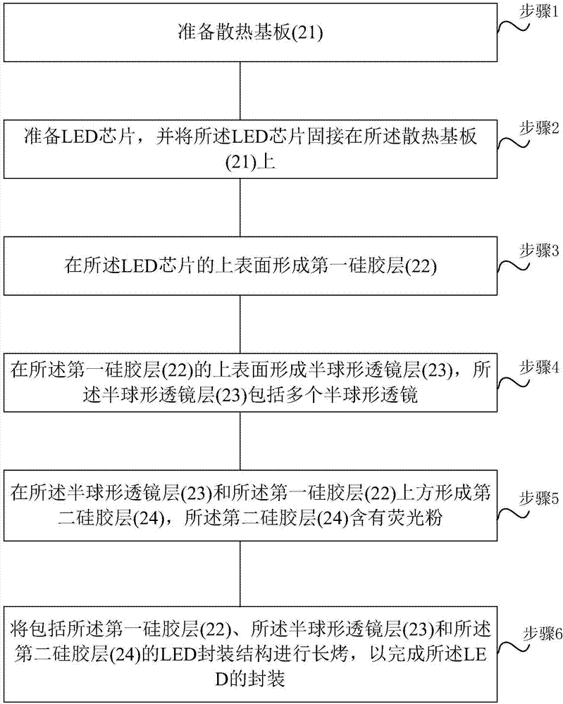
[0050] An embodiment of the present invention provides an LED packaging method, which includes,

[0051] Step 1, preparing the heat dissipation substrate 21;

[0052] Step 2, preparing LED chips, and fixing the LED chips on the heat dissipation substrate 21;

[0053] Step 3, forming a first silica gel layer 22 on the upper surface of the LED chip;

[0054] Step 4, forming a hemispherical lens layer 23 on the upper surface of the first silica gel layer 22, the hemispherical lens layer 23 comprising a plurality of hemispherical lenses;

[0055] Step 5, forming a second silica gel layer 24 above the hemispherical lens layer 23 and the first silica gel layer 22, the second silica gel layer 24 containing fluorescent powder;

[0056] Step 6, long-baking the LED package structure including the first silicone layer 22 , the hemispherical lens layer 23 and the second silicone layer 24 to complete the package of the LED.

[0057] Further, the LED chip is an aluminum gallium nitride u...

Embodiment 2

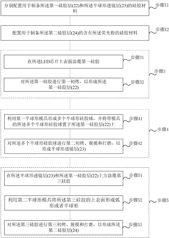
[0085] Please refer to figure 1 , figure 1 The flow chart of the LED packaging method provided by the embodiment of the present invention; wherein, on the basis of the above-mentioned embodiments, the LED packaging method provided by the embodiment of the present invention is introduced in detail, and the specific steps are as follows:

[0086] Step 1, preparing the heat dissipation substrate 21;

[0087] Step 11, selecting the heat dissipation substrate 21;

[0088] Specifically, a heat dissipation substrate 21 with a thickness D of 0.5-10mm and a solid iron plate is selected, and the heat dissipation substrate 21 is cut to a required size. The width W of the substrate is cut according to actual needs, which is not limited here.

[0089] Step 12, cleaning the heat dissipation substrate 21;

[0090] Specifically, clean the stains on the heat dissipation substrate 21, especially the oil stains;

[0091] Step 13, drying the heat dissipation substrate 21;

[0092] Specifical...


PUM


Abstract

The invention relates to an LED package method. The LED package method comprises the steps of preparing a cooling substrate (21); preparing an LED chip, fixedly connecting the LED chip onto the cooling substrate (21); forming a first silica gel layer (22) on an upper surface of the LED chip; forming a semi-spherical lens layer (23) on an upper surface of the first silica gel layer (22), wherein the semi-spherical lens layer (23) comprises a plurality of semi-spherical lenses; forming a second silica gel layer (24) above the semi-spherical lens layer (23) and the first silica gel layer (22), wherein the second silica gel layer (24) contains fluorescent powder; and baking an LED package structure comprising the first silica gel layer (22), the semi-spherical lens layer (24) and the second silica gel layer (24) for a long time so as to complete package of an LED. According to the LED package method disclosed by the embodiment of the invention, the semi-spherical lens layer is arranged between the first silica gel layer and the second silica gel layer, the fluorescent powder is arranged in the second silica gel layer, so that light beams are more concentrated and uniformly irradiate, moreover, the fluorescent powder is prevented from being in direct contact with the LED chip, and the light extraction efficiency is improved.

Description

technical field [0001] The invention belongs to the technical field of photoelectric devices, and in particular relates to an LED packaging method. Background technique [0002] Light Emitting Diode (LED) is a solid-state semiconductor device that can convert electrical energy into visible light. It is widely used in display screens, traffic signals, display light sources, automotive lights, LED backlights, and lighting sources. . [0003] However, in practical application, those skilled in the art find that the prior art has at least the following technical problems: [0004] 1. Since the light emitted by the LED light source is generally distributed in a divergent manner, the light is not concentrated, and the secondary shaping through the external lens increases the production cost; [0005] 2. Phosphor powder is generally directly coated on the surface of the chip. The high temperature generated by the LED chip reduces the quantum efficiency of the phosphor powder. In ...

Claims


Application Information

Patent Timeline
Patent Type & Authority Applications(China)
IPC IPC(8): H01L33/48H01L33/50H01L33/56H01L33/58
CPCH01L33/48H01L33/507H01L33/56H01L33/58H01L2933/0033H01L2933/0041H01L2933/005H01L2933/0058
Inventor 张亮
Owner YANGZHOU HUACAI OPTO ELECTRONICS
Why Eureka
Try Eureka