LED packaging structure and high-concentration LED lamp

A technology of LED packaging and LED chips, applied in semiconductor devices, electrical components, circuits, etc., can solve the problems of decreasing quantum efficiency, reducing luminous efficiency, and dispersion of LED light source distribution, and achieve the effect of improving luminous dispersion.

Inactive Publication Date: 2018-05-08
XIAN CREATION KEJI CO LTD
View PDF4 Cites 0 Cited by
  • Summary
  • Abstract
  • Description
  • Claims
  • Application Information

AI Technical Summary

Problems solved by technology

[0004] LEDs that use the above method to emit light have the following defects: the distribution of light emitted by the LED light source is relatively scattered, and the illumination brightness of the light source is not good. It often needs to be shaped by an external lens to meet the brightness requirements, which greatly increases the production cost of the LED; The powder is directly coated on the surface of the chip, and the chip absorbs the scattered light, which reduces the luminous efficiency. Moreover, the high temperature of the chip will reduce the quantum efficiency of the phosphor powder, which will affect the lumen efficiency of the LED light source, which will easily lead to a decrease in light intensity. A series of problems such as spectral shift and accelerated aging of the chip reduce the service life of the LED light source

Method used


Image

  • LED packaging structure and high-concentration LED lamp
  • LED packaging structure and high-concentration LED lamp
  • LED packaging structure and high-concentration LED lamp

Examples


Embodiment 1

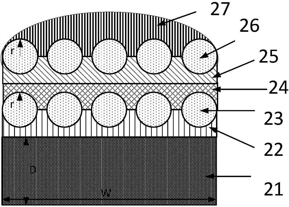
[0039] See figure 1 , figure 1 A schematic diagram of an LED packaging structure provided by an embodiment of the present invention, the packaging structure includes:

[0040] heat sink (21);

[0041] LED chips, arranged on the heat sink (21);

[0042] A first silica gel layer (22), coated on the LED chip and the heat sink (21);

[0043] A first lens layer (23), prepared on the first silica gel layer (22);

[0044] A second silica gel layer (24) and a third silica gel layer (25), which are successively arranged on the first lens layer (23);

[0045] A second lens layer (26), arranged on the third silica gel layer (25);

[0046] The fourth silica gel layer (27) is arranged on the second lens layer (26).

[0047] Further, on the basis of the above embodiment, the first silica gel layer (22) does not contain fluorescent powder, the first lens layer (23), the second silica gel layer (24), the third silica gel layer At least one of the layer (25), the second lens layer (26) ...

Embodiment 2

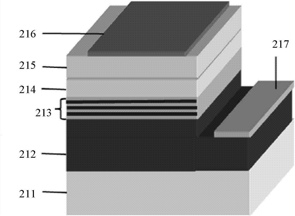
[0060] This embodiment further describes the LED package structure and its manufacturing method in the embodiment.

[0061] See Figure 4 , Figure 4 A schematic diagram of an LED packaging process flow provided by an embodiment of the present invention, the method includes:

[0062] Select the LED chip;

[0063] Welding the LED chip on the heat sink (21), placing the heat sink on the bracket;

[0064] A multi-layer silica gel layer is formed on the LED chip to realize the packaging of the LED chip, wherein the silica gel layer in contact with the LED chip in the multi-layer silica gel layer does not contain fluorescent powder.

[0065] In this embodiment, the silica gel layer in direct contact with the LED chip does not contain phosphor, and the phosphor is placed in other silica gel layers that do not directly contact the LED chip, avoiding direct contact between the phosphor powder and the LED chip. The reason for the implementation is: the chip has an absorption effect...


PUM


Abstract

The invention relates to an LED packaging structure and a high-concentration LED lamp. The LED packaging structure comprises heat sink (21), an LED chip, a first silica gel layer (22), a first lens layer (23), a second silica gel layer (24), a third silica gel layer (25), a second lens layer (26) and a fourth silica gel layer (27), wherein the LED chip is arranged on the heat sink (21); the silicagel layer (22) coats the LED chip and the heat sink (21); the first lens layer (23) is prepared on the first silica gel layer (22); the second silica gel layer (24) and the third silica gel layer (25) are sequentially arranged on the first lens layer (23); the second lens layer (26) is arranged on the third silica gel layer (25); and the fourth silica gel layer (27) is arranged on the second lenslayer (26). According to the LED packaging structure provided by the invention, fluorescent powder is separated from the LED chip, so that the problem that the quantum efficiency of the fluorescent powder is reduced due to high temperature is solved; and silica gel in contact with the LED chip is high-temperature resistant silica gel, so that the problem that the light transmittance is reduced due to ageing and yellowing of the silica gel is solved.

Description

technical field [0001] The invention belongs to the technical field of semiconductors, and in particular relates to an LED packaging structure and a high-concentration LED lamp. Background technique [0002] LED (Light Emitting Diode), light-emitting diode, is a solid-state semiconductor device that can directly convert electricity into light. The practicality and commercialization of high-performance LEDs have brought about a new revolution in lighting technology. The pixel light composed of multiple ultra-high-brightness red, blue, and green LEDs can not only emit various colors of light with continuously adjustable wavelengths, but also emit white light with a brightness of tens to one hundred candlepower as a lighting source. For incandescent lamps and LED solid-state lighting lamps with the same luminance, the power consumption of the latter only accounts for 10%-20% of the former. [0003] Most of the white LEDs currently produced are made by covering a layer of ligh...

Claims


Application Information

Patent Timeline
Patent Type & Authority Applications(China)
IPC IPC(8): H01L33/50H01L33/54H01L33/56H01L33/58
CPCH01L33/507H01L33/502H01L33/54H01L33/56H01L33/58
Inventor 左瑜
Owner XIAN CREATION KEJI CO LTD
Why Eureka
Try Eureka