
OPC (optical proximity correction) Method

A processing method and graphics technology, applied in special data processing applications, optics, instruments, etc., can solve the problems of shrinking graphics size, increasing the number of hot spots, and consuming a lot of OPC engineer time OPC calculation time.

Active Publication Date: 2018-05-08
SHANGHAI HUALI MICROELECTRONICS CORP
View PDF9 Cites 3 Cited by
  • Summary
  • Abstract
  • Description
  • Claims
  • Application Information

AI Technical Summary

Problems solved by technology

[0009] It can be seen from the above that the processing of hotspots in the existing method needs to consume a lot of OPC engineer time, a lot of OPC computing time and a lot of software and hardware resources, and with the improvement of integration and the reduction of graphic size, the number of hotspots will increase

Method used


Image

  • OPC (optical proximity correction) Method
  • OPC (optical proximity correction) Method
  • OPC (optical proximity correction) Method

Examples


Embodiment O

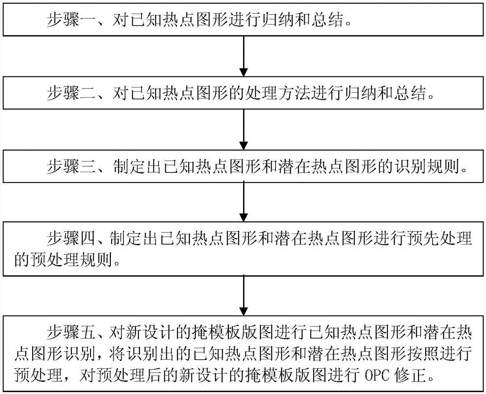
[0061] Such as figure 1 Shown is the flowchart of the OPC correction method of the embodiment of the present invention; the OPC correction method of the embodiment of the present invention comprises the following steps:

[0062] Step 1. Taking the hotspot patterns appearing in the OPC-corrected mask layout as known hotspot patterns and summarizing the known hotspot patterns.

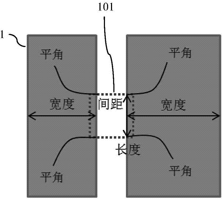
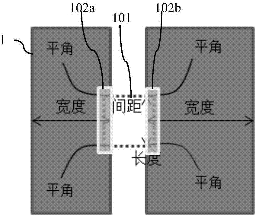
[0063] Such as Figure 2A Shown is the layout of the known hotspot graphics corresponding to the first short-circuit hotspot; Figure 3A Shown is the layout of the known hotspot graphics corresponding to the second short-circuit hotspot; Figure 4A As shown in , it is the layout of the known hotspot graphics corresponding to the connection error hotspots of the upper and lower layers; Figure 5A Shown is the layout of known hotspot graphics corresponding to open circuit hotspots; the steps of inducing and summarizing the known hotspot graphics include:

[0064] Classify and determine the parameters o...


PUM


Abstract

The invention discloses an OPC (optical proximity correction) method, comprising the steps of I, summarizing known hotspot figures and making a conclusion; II, summarizing processing methods of the known hotspot figures, and making a conclusion; III, formulating recognition rules for the known hotspot figures and potential hotspot figures; IV, formulating preprocessing rules to preprocessing the known hotspot figures and potential hotspot figures; V, subjecting a newly designed mask layout to recognition of known hotspot figures and potential hotspot figures, preprocessing the recognized knownhotspot figures and potential hotspot figures, and subjecting the preprocessed newly-designed mask layout to OPC. The OPC method has the advantages that the quantity of hotspots subjected to OPC canbe decreased or eliminated, and therefore, time of OPC engineers, OPC operation time and software-hardware resources can be saved.

Description

technical field [0001] The invention relates to a semiconductor integrated circuit manufacturing method, in particular to an optical proximity correction (Optical Proximity Correction, OPC) correction method. Background technique [0002] In the photolithography process of semiconductor integrated circuits, the graphic structure of the circuit is first defined on the mask layout, and then the graphic structure on the mask layout is transferred to the photoresist formed on the surface of the wafer by photolithography to form a photolithographic process. glue graphics. During the photolithography process, when the size of the pattern and the size of the wavelength of the lithography are close to or even smaller, the pattern exposed on the photoresist and the pattern on the mask template will be caused by light interference, diffraction and development. Inconsistency results in distortion of the Optical Proximity Effect (OPE). Therefore, in order to form the required pattern ...

Claims


Application Information

Patent Timeline
Patent Type & Authority Applications(China)
IPC IPC(8): G06F17/50G03F1/36
CPCG03F1/36G06F30/398
Inventor 王丹毛智彪于世瑞
Owner SHANGHAI HUALI MICROELECTRONICS CORP
Learn More