Current sampling circuit applied to boost-buck circuit and control method thereof
A current sampling and sampling current technology, which is applied in the direction of measuring current/voltage, only measuring current, and controlling/regulating systems, etc., can solve the problems of increasing system cost and increasing power consumption, so as to avoid current peaks, reduce power consumption, and reduce Effect of chip pin count
- Summary
- Abstract
- Description
- Claims
- Application Information
AI Technical Summary
Problems solved by technology
Method used
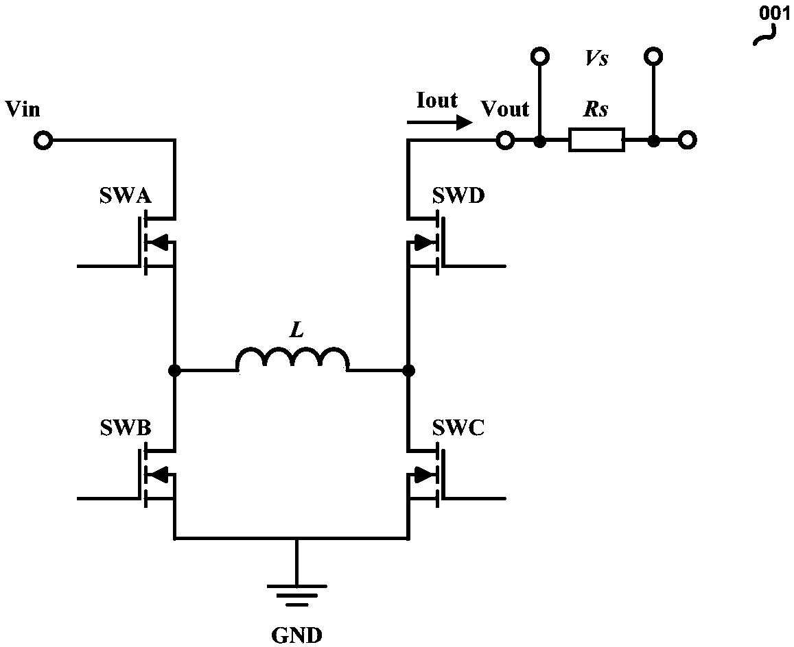
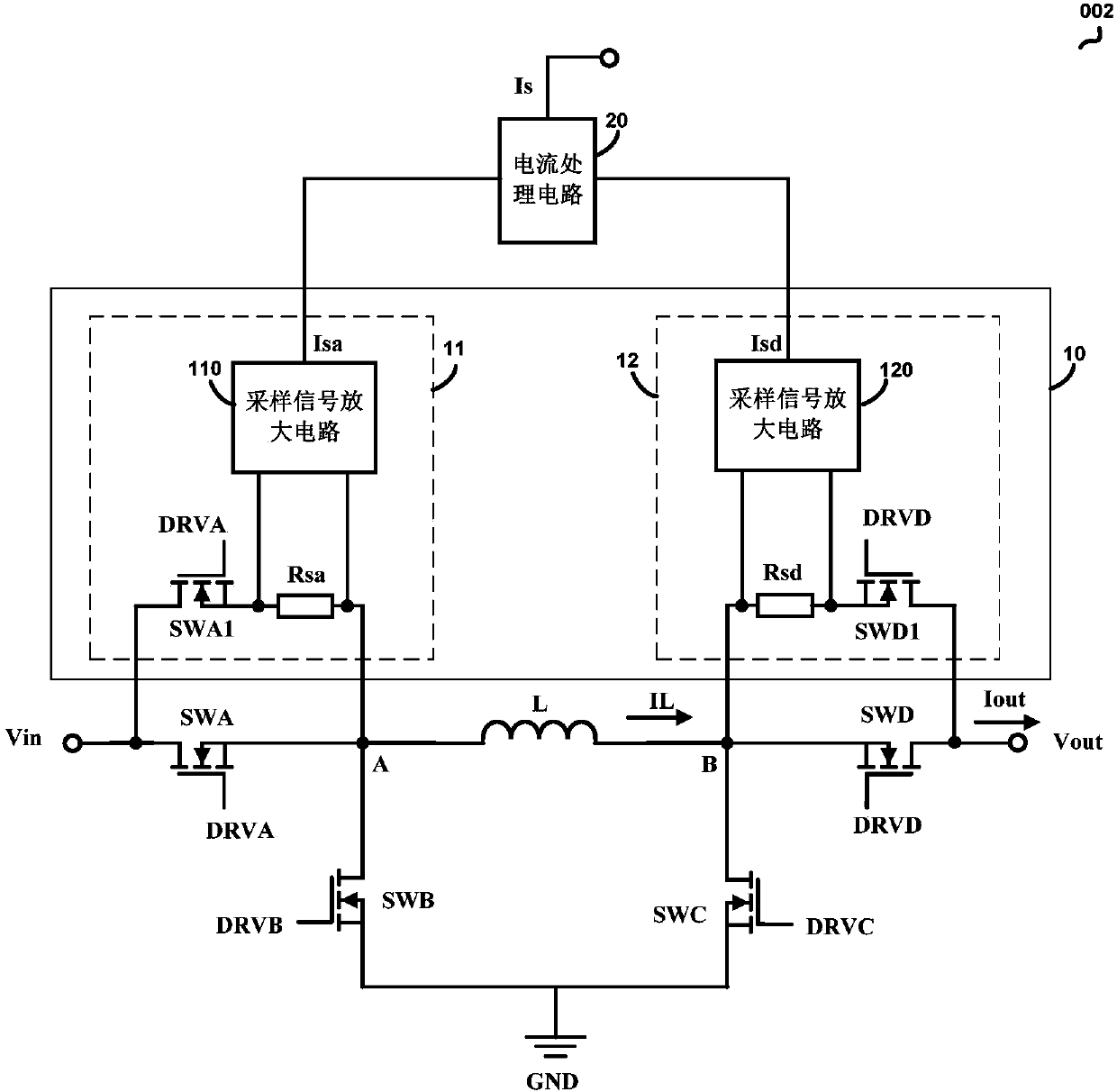
Image


Examples
Embodiment Construction
[0019] Specific embodiments of the present invention will be described in detail below, and it should be noted that the embodiments described here are only used for illustration, and are not intended to limit the present invention. In the following description, numerous specific details are set forth in order to provide a thorough understanding of the present invention. It will be apparent, however, to one of ordinary skill in the art that these specific details need not be employed to practice the present invention. In other instances, well-known circuits, materials or methods have not been described in detail in order to avoid obscuring the present invention.
[0020] Throughout this specification, reference to "one embodiment," "an embodiment," "an example," or "example" means that a particular feature, structure, or characteristic described in connection with the embodiment or example is included in the present invention. In at least one embodiment. Thus, appearances of ...
PUM
 Abstract
Description
Claims
Application Information
 - R&D
- Intellectual Property
- Life Sciences
- Materials
- Tech Scout
- Unparalleled Data Quality
- Higher Quality Content
- 60% Fewer Hallucinations
Browse by: Latest US Patents, China's latest patents, Technical Efficacy Thesaurus, Application Domain, Technology Topic, Popular Technical Reports.
© 2025 PatSnap. All rights reserved.Legal|Privacy policy|Modern Slavery Act Transparency Statement|Sitemap|About US| Contact US: help@patsnap.com