A wavelength-tunable electroluminescent device
A technology of electroluminescent devices and light-emitting devices, which is applied in the direction of electric solid-state devices, electrical components, semiconductor devices, etc., can solve the problem that the emission wavelength can no longer be changed, and achieve the effect of high color rendering index, simple process and few processes
- Summary
- Abstract
- Description
- Claims
- Application Information
AI Technical Summary
Problems solved by technology
Method used
Image
Examples
Embodiment 1
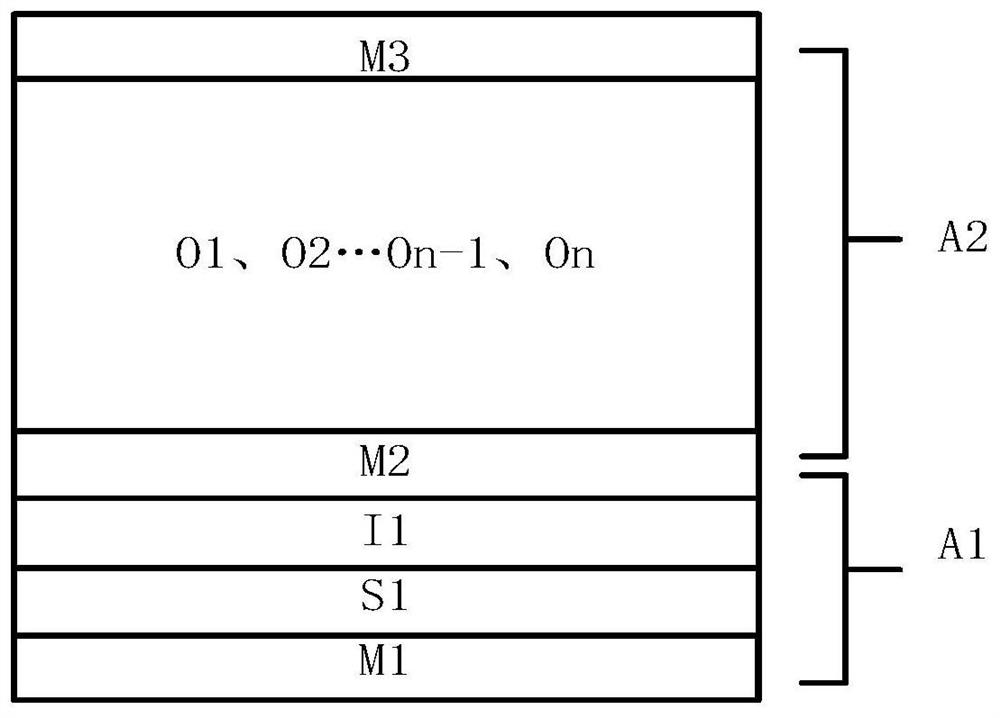
[0048] Such as figure 2 As shown, a wavelength-modulatable electroluminescent device of the present invention is composed of two units A1 and A2. A1 is a voltage modulation unit composed of a metal electrode M1, a semiconductor material S1, a dielectric material I1, and a metal electrode M2. M1 and M2 are continuous electrode film materials. M1 is an Au film with a thickness of 40nm; the semiconductor material S1 is a TiN film with a thickness of 10nm; the I1 layer is SiO 2 thin film with a thickness of 8nm; the M2 layer is an Au thin film with a thickness of 10nm. A2 is a top-emitting organic electroluminescent device, the bottom electrode is the common electrode M2 of the voltage modulation unit, O1 is the electrode modification layer, which is composed of 2nm Ag2O, and O2 is the hole injection layer, which is composed of 22.5nm m-MTDATA; O3 is the electron blocking layer, which is composed of 5nm NPB film; O4 is the light emitting layer, which is composed of 15nm DPVBi...
Embodiment 2
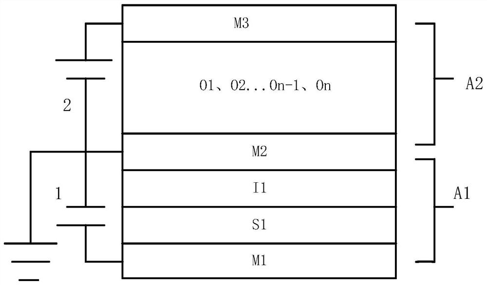
[0052] Such as image 3 As shown, a wavelength-modulatable electroluminescent device of the present invention is composed of two units A1 and A2, A1 is a voltage modulation unit, which is composed of a grid-shaped metal electrode M1, a semiconductor material S1, a dielectric material I1, and a metal electrode M2. . M2 is a continuous electrode film material. The gate electrode M1 is an Au electrode with a thickness of 40nm and a width of 500nm, and each Au gate electrode is separated by 1um, and voltage can be applied independently. The semiconductor material S1 is a TiN film with a thickness of 10nm; the I1 layer is SiO 2 thin film with a thickness of 8nm; the M2 layer is an Au thin film with a thickness of 10nm. A2 is a top-emitting organic electroluminescent device, the bottom electrode is the common electrode M2 of the voltage modulation unit, O1 is the electrode modification layer, which is composed of 2nm Ag2O, and O2 is the hole injection layer, which is composed o...
PUM
| Property | Measurement | Unit |
|---|---|---|
| thickness | aaaaa | aaaaa |
| thickness | aaaaa | aaaaa |
| thickness | aaaaa | aaaaa |
Abstract
Description
Claims
Application Information
 - R&D
- Intellectual Property
- Life Sciences
- Materials
- Tech Scout
- Unparalleled Data Quality
- Higher Quality Content
- 60% Fewer Hallucinations
Browse by: Latest US Patents, China's latest patents, Technical Efficacy Thesaurus, Application Domain, Technology Topic, Popular Technical Reports.
© 2025 PatSnap. All rights reserved.Legal|Privacy policy|Modern Slavery Act Transparency Statement|Sitemap|About US| Contact US: help@patsnap.com


