
A kind of otp memory and its data writing and reading method, security chip

A data writing and memory technology, applied in the field of memory and information security, can solve the problem that the key data is easily obtained illegally, and achieve the effect of increasing the difficulty of identification, increasing the difficulty, and improving security

Active Publication Date: 2020-12-29
SHENZHEN GRADUATE SCHOOL TSINGHUA UNIV
View PDF6 Cites 0 Cited by
  • Summary
  • Abstract
  • Description
  • Claims
  • Application Information

AI Technical Summary

Problems solved by technology

Therefore, the key data is easily obtained illegally

Method used


Image

  • A kind of otp memory and its data writing and reading method, security chip
  • A kind of otp memory and its data writing and reading method, security chip
  • A kind of otp memory and its data writing and reading method, security chip

Examples


specific Embodiment approach 1

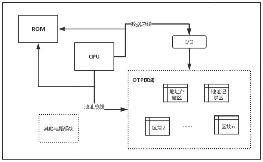
[0040] Generally, a security chip at least includes an on-chip CPU, ROM, a key storage area (usually an OTP array), and related processing circuit modules. The ROM usually stores the processing code and data for the on-chip CPU to operate the logic of the chip, such as logical processing such as analyzing and extracting the key. The key storage area, that is, the OTP memory generally stores key data. The process of improving the security protection of the key data in the security chip proposed by the present invention includes the segmentation and isolation of the OTP storage area, and the randomization of reading and writing of the storage area.

[0041] The writing of key data is realized through chip programming. When programming, the anti-fuse structure is broken down by a high-voltage signal, and the state of the OTP bit is changed to write data 0 or 1. Once the data is written into the bit, it will not be able to be programmed, otherwise the bit will be damaged. . Whe...

specific Embodiment approach 2

[0053] The difference between this specific embodiment and the first embodiment is that: when writing data in each OTP small block, it is further restricted to write in a segmented and encapsulated manner, thereby further improving the security of data storage.

[0054] In this embodiment, when writing data, a complete piece of input data is decomposed and randomly stored in each address segment in a small block. The traditional data storage method is to directly write all the data into a continuous segment starting with a certain address. Although this method is more convenient in reading and writing data, illegal personnel can easily obtain the key data through methods such as bus detection, and the storage security is not high. In this specific embodiment, any segment of input data is decomposed and stored in a random address segment, and the same data as that at the time of storage is returned when read. For the user, the processing logic is completely closed, and this da...


PUM


Abstract

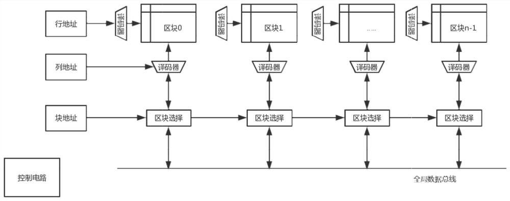
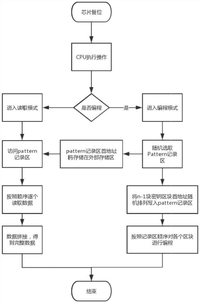
The invention discloses an OTP memory, data writing and reading methods thereof and a security chip. The data writing method of the OTP memory includes the following steps: S1, carrying out block dividing on the OTP memory in physical space to form n+1 blocks of storage areas, wherein n is a positive integer which is greater than 1, and the n+1 blocks of storage areas include n blocks of data storage areas and one block of address storage area which is always in a readable state; S2, generating a random sequence through a random-number generator, randomly selecting one block from the n blocksof data storage areas according to the random sequence, and defining the same as an address recording area; S3, sequentially writing first addresses of n-1 blocks of data storage areas into the address recording area according to a random order, and writing to-be-stored data in each block of data storage area according to a successive order of writing; and S4, writing a first address of the address recording area into the address storage area which is always in the readable state. According to the data writing method and reading method of the invention, difficulty of acquiring the data, whichare stored in the memory, by a cracker can be increased, and storage security can be improved.

Description

【Technical field】 [0001] The invention relates to the field of memory and information security, in particular to a data writing and reading method of an OTP memory. 【Background technique】 [0002] OTP is a one-time programmable memory type. Its main feature is that it can only be programmed once, so it has the characteristics of protecting important data, so it is widely used in the key storage area of ​​security chips. A security chip refers to an integrated chip that can store keys and characteristic data and has an independent processing unit and storage area. It is widely used in security fields such as identity authentication and digital signature. Although the security chip has sufficient confidentiality, the development of reverse engineering in recent years has reached the point where it is enough to break through the general security chip. [0003] Reverse engineering reverse acquisition methods for chips mainly include physical grinding and focused ion beam proces...

Claims


Application Information

Patent Timeline
Patent Type & Authority Patents(China)
IPC IPC(8): G06F3/06
CPCG06F3/062G06F3/064G06F3/0679G06F21/79
Inventor 王兴军赵海峰
Owner SHENZHEN GRADUATE SCHOOL TSINGHUA UNIV
Learn More