A kind of manufacturing method of flash memory wafer

A manufacturing method and wafer technology, applied in the direction of transistors, semiconductor/solid-state device manufacturing, diodes, etc., can solve problems affecting product storage performance, weakening the coupling rate of control gate and floating gate, etc., and achieve the effect of realizing height and adjustment

Active Publication Date: 2020-05-15
SHANGHAI HUALI MICROELECTRONICS CORP
View PDF3 Cites 0 Cited by
  • Summary
  • Abstract
  • Description
  • Claims
  • Application Information

AI Technical Summary

Problems solved by technology

However, this change in the storage area will weaken the coupling ratio between the control gate and the floating gate, thereby affecting the storage performance of the product

Method used


Image

  • A kind of manufacturing method of flash memory wafer
  • A kind of manufacturing method of flash memory wafer
  • A kind of manufacturing method of flash memory wafer

Examples


Embodiment Construction

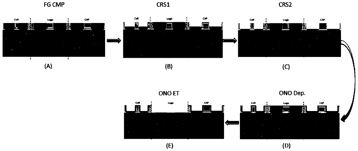
[0034] In order to make the purpose, technical solution and advantages of the present invention clearer, the specific implementation manners of the present invention will be further described in detail below in conjunction with the accompanying drawings.

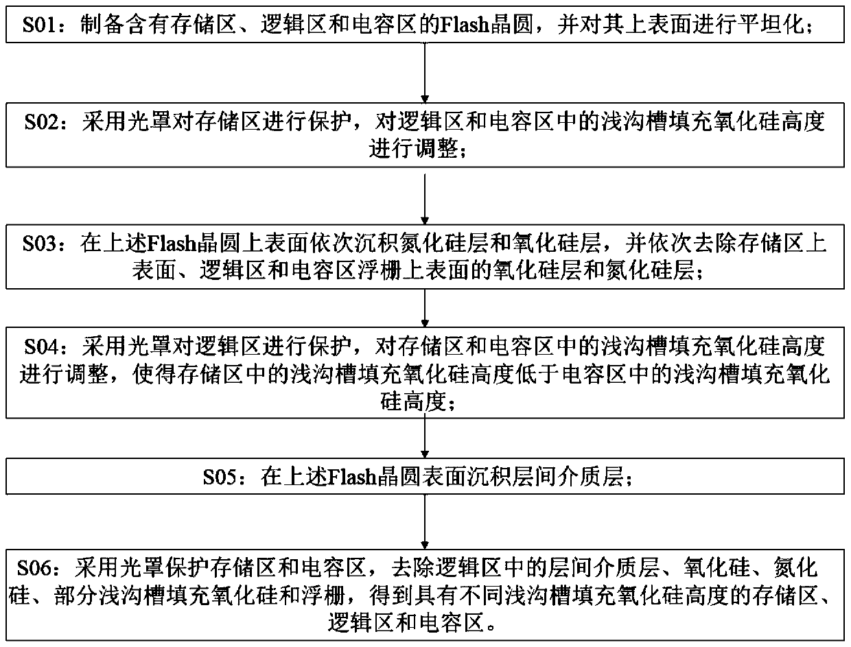
[0035] as attached image 3 And attached Figure 4 As shown, a kind of preparation method of flash memory wafer provided by the present invention comprises the following steps:

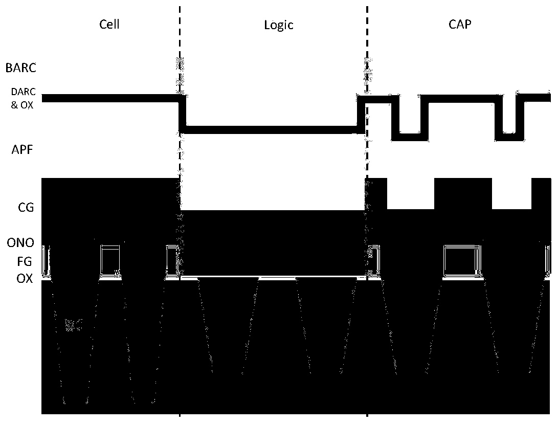
[0036] S01: If Figure 4 As shown in A, a flash memory wafer containing a storage area, a logic area, and a capacitor area is prepared, and its upper surface is planarized, wherein the storage area, the logic area, and the capacitor area all include shallow trench isolation and an active area, and the shallow The trench isolation is located in the gap of the active area, and there is a floating gate above the active area. The shallow trench isolation contains shallow trench filling silicon oxide, and the planarized shallow trench filling silicon o...


PUM


Abstract

The invention discloses a manufacturing method of a Flash wafer, comprising the following steps: S01: preparing a Flash wafer containing a storage area, a logic area and a capacitance area, and planarizing the upper surface thereof; S02: preparing the logic area and the capacitance area The height of the shallow trench filling silicon oxide in the region is adjusted; S03: Deposit a silicon nitride layer and a silicon oxide layer on the upper surface of the above-mentioned Flash wafer in sequence, and remove the upper surface of the storage region, the logic region and the upper surface of the floating gate of the capacitor region in sequence The silicon oxide layer and silicon nitride layer; S04: Adjust the height of the shallow trench filling silicon oxide in the storage area and the capacitor area to make it different; S05: Deposit an interlayer dielectric layer on the surface of the above-mentioned Flash wafer; S06: A photomask is used to protect the storage area and the capacitor area, and the remaining part of the logic area is removed to obtain the storage area, the logic area and the capacitor area with different heights of shallow trenches filled with silicon oxide. The invention can realize the independent adjustment of the height of silicon oxide filled in shallow trenches in the capacitor region.

Description

technical field [0001] The invention relates to the field of semiconductor manufacturing, in particular to a method for manufacturing a flash memory wafer. Background technique [0002] For flash memory products that use floating gates to store information, a capacitor region is usually added to the product. The film layer deposited on the newly added capacitance area is the same as the film layer of the control gate in the storage area, and there are floating gates above the active area in both the capacitance area and the storage area, and the floating gate is polysilicon. However, there is no floating gate on the shallow trench isolation in the capacitance area, and the width of the shallow trench isolation is larger than that in the storage area. Therefore, the subsequent process cannot control the polysilicon growth as in the storage region, so that the shallow trench isolation in the capacitor region is the same as the total thickness of the polysilicon layer on the a...

Claims


Application Information

Patent Timeline
Patent Type & Authority Patents(China)
IPC IPC(8): H01L27/11517
CPCH10B41/00H01L21/76229H01L27/0629H10B41/42H10B41/44H01L21/76224H10B41/50
Inventor 许鹏凯乔夫龙王一
Owner SHANGHAI HUALI MICROELECTRONICS CORP
Why Eureka
Try Eureka