Integrated circuit semi-custom rear end ECO (electron-coupled oscillator) design method

A technology of integrated circuits and design methods, applied in the field of design automation EDA in the integrated circuit design industry, can solve the problems of poor design quality and long iteration time, reduce the number of design iterations, avoid invalid work, improve versatility and integrity Effect

Inactive Publication Date: 2018-03-13
嘉兴倚韦电子科技有限公司
View PDF3 Cites 0 Cited by
  • Summary
  • Abstract
  • Description
  • Claims
  • Application Information

AI Technical Summary

Problems solved by technology

[0003] Therefore, the ECO design stage of chip design is an important part of the entire semi-custom back-end design process, but the current conventional ECO design method has defects, mainly due to problems such as poor design quality and too long iteration time

Method used


Image

  • Integrated circuit semi-custom rear end ECO (electron-coupled oscillator) design method
  • Integrated circuit semi-custom rear end ECO (electron-coupled oscillator) design method
  • Integrated circuit semi-custom rear end ECO (electron-coupled oscillator) design method

Examples


Embodiment Construction

[0027] The invention discloses an ECO design method for integrated circuit semi-customized back-end design. The specific implementation of the invention will be further described below in combination with preferred embodiments.

[0028] It is worth noting that those skilled in the art should understand that the ECO involved in the patent application of the present invention is defined as Engineering Change Order; the RTL involved in the patent application of the present invention is positioned as Resistor Transistor Logic.

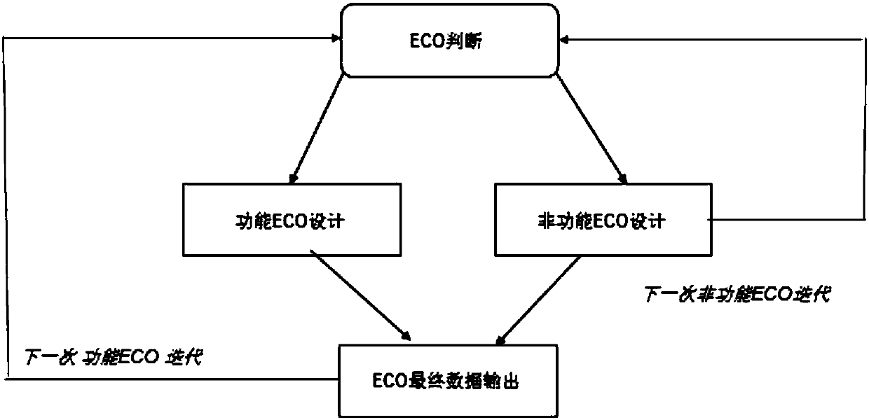
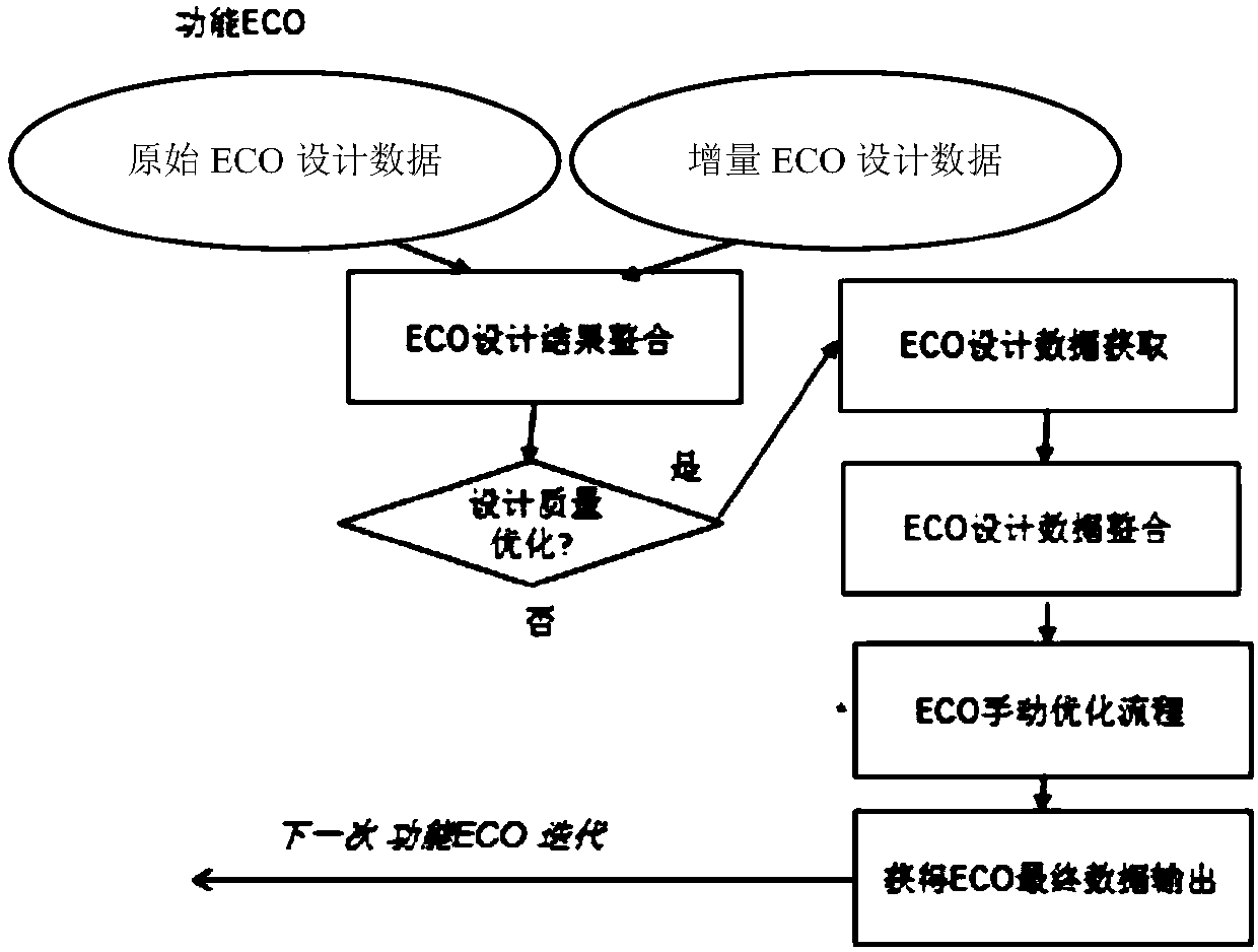
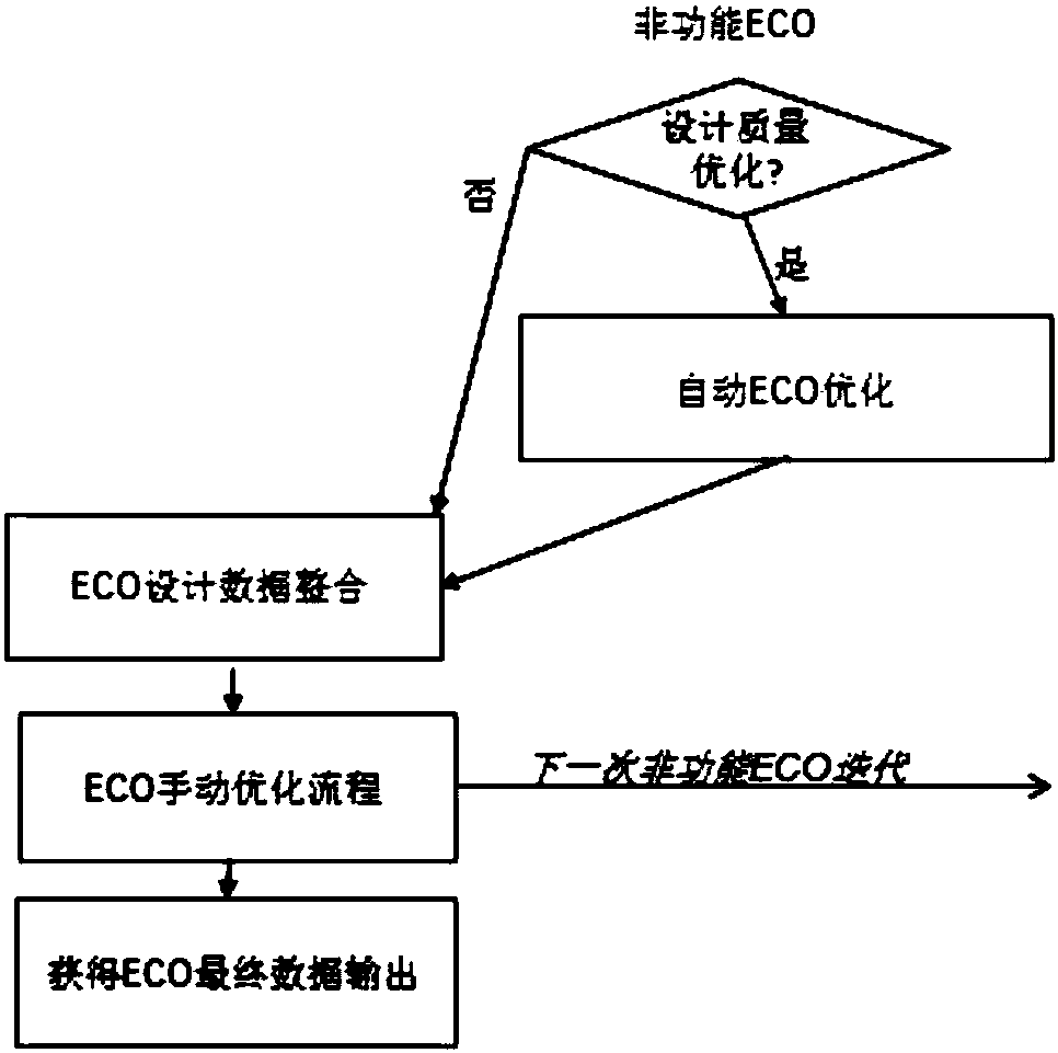
[0029] see attached figure 1 , figure 1 The ECO design method for semi-custom back-end design of integrated circuits is shown. Preferably, the integrated circuit semi-custom back-end design ECO design method includes the following steps:

[0030] Step S1: The back-end design tool distinguishes the ECO design requirements into functional ECO design or non-functional ECO design. If it is a functional ECO design, perform step S2, and if it is a non-function...


PUM


Abstract

The invention discloses an integrated circuit semi-custom rear end ECO (electron-coupled oscillator) design method which includes the steps: S1 distinguishing an ECO design requirement into functionalECO design or non-functional ECO design by a rear end design tool, executing a step S2 if the ECO design requirement is the functional ECO design, and executing a step S3 if the ECO design requirement is the non-functional ECO design; S2 judging whether optimization is needed or not according to original ECO data and incremental ECO data, sequentially executing automatic optimization, manual optimization and outputting of a functional ECO design result if optimization is needed, and sequentially executing manual optimization and outputting of the functional ECO design result if not. Accordingto the integrated circuit semi-custom rear end ECO design method, integrated chip rear end design efficiency is improved, invalid working is effectively avoided, design iteration frequency is reduced, a chip design period is shortened, and the method is suitable for rear end design projects with different design requirements and has good universality and integrity.

Description

technical field [0001] The invention belongs to the technical field of design automation EDA in the integrated circuit design industry, and in particular relates to an ECO design method for semi-customized back-end design of integrated circuits. Background technique [0002] In the whole design process of integrated chips, designers usually need to continuously verify the design. For early design problems, designers can solve them by modifying the RTL code. However, in the later stage of design, such as nearing the final signoff (signoff), it needs to be implemented through an engineering change order (ECO, Engineering Change Order) technology. [0003] Therefore, the ECO design stage of chip design is an important part of the entire semi-custom back-end design process, but the current conventional ECO design method has defects, mainly due to poor design quality and too long iteration time. Therefore, it is necessary to propose an efficient ECO design method to improve the...

Claims


Application Information

Patent Timeline
Patent Type & Authority Applications(China)
IPC IPC(8): G06F17/50
CPCG06F30/39
Inventor 徐靖
Owner 嘉兴倚韦电子科技有限公司
Why Eureka
Try Eureka