Rapid-locking low-jitter clock data recovery circuit based on double loops

A clock data recovery, low jitter technology, applied in the direction of automatic power control, electrical components, etc., can solve the problem that the clock data recovery circuit cannot have fast locking speed at the same time, and achieve low power consumption, low jitter, and simple structure. Effect

Active Publication Date: 2018-02-09
HARBIN INST OF TECH
View PDF9 Cites 2 Cited by
  • Summary
  • Abstract
  • Description
  • Claims
  • Application Information

AI Technical Summary

Problems solved by technology

[0004] The purpose of the present invention is to solve the problem that the existing double-loop clock data recovery circuit cannot have fast locking speed and small jitter at the same time, thereby providing a clock data recovery circuit based on double-loop fast locking and low jitter

Method used


Image

  • Rapid-locking low-jitter clock data recovery circuit based on double loops
  • Rapid-locking low-jitter clock data recovery circuit based on double loops
  • Rapid-locking low-jitter clock data recovery circuit based on double loops

Examples


specific Embodiment approach 1

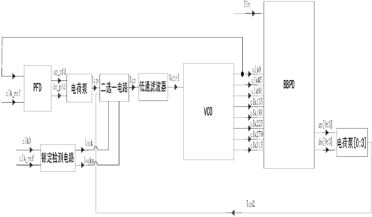
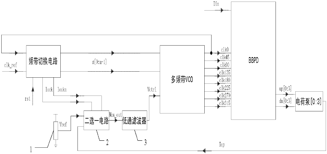
[0027] Specific implementation mode one: combine figure 2 and image 3 Describe this embodiment in detail, the clock data recovery circuit based on double-loop fast locking and low jitter described in this embodiment includes a frequency band switching circuit, a multi-band VCO, BBPD, 4 charge pumps, a low-pass filter, and a resistor divider circuit and alternative circuit;

[0028] The circuit adjusts the frequency band of the multi-band VCO through a frequency-locked loop to achieve frequency locking, and adjusts the control voltage of the multi-band VCO through a phase-locked loop to achieve phase locking;

[0029] Frequency-band switching circuit, multi-band VCO, resistor divider circuit, two-choice circuit and low-pass filter form a frequency-locked loop;

[0030] One-of-two circuit, low-pass filter, multi-band VCO, BBPD, and 4 charge pumps form a phase-locked loop;

[0031] The reference clock input terminal of the frequency band switching circuit is connected to the...

Embodiment

[0047] The clock data recovery circuit is 1 / 4 rate, the input data frequency is 12.5GHz, the reference clock frequency is 3.125GHz, the multi-band VCO has 8 frequency bands in total, and the output 8-phase clock is "011" in the frequency band, and the control voltage is about 3.125GHz clock is output at 580mV, the result of resistor division is 600mV, and the power supply voltage is 1.2V.

[0048] Simulation results such as Figure 4 shown.

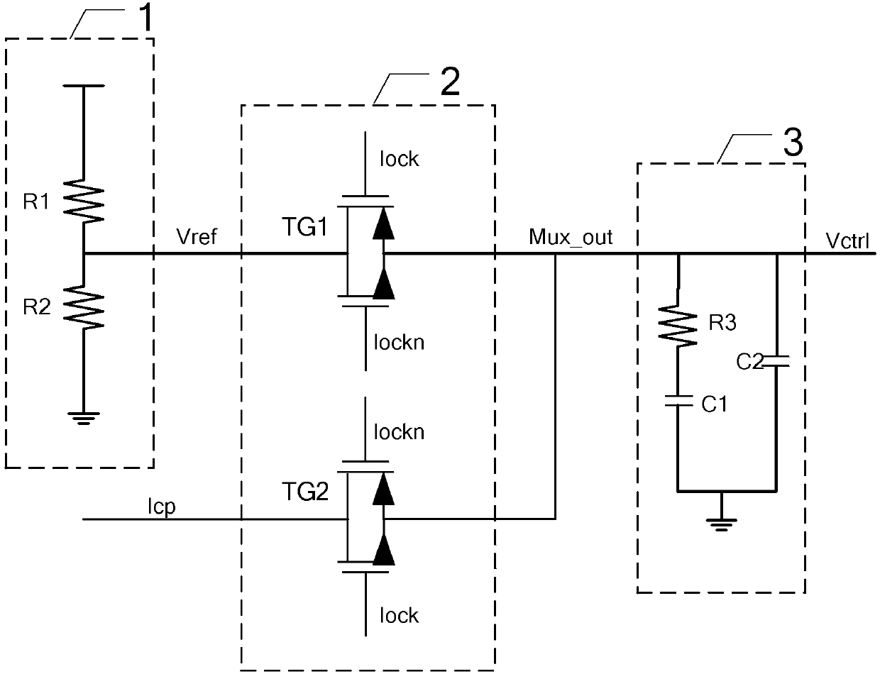
[0049] Initial state: The state after reset is the initial state. At this time, the frequency band control word s[0:2] of the multi-band VCO is "000", the lock signal is "0", the lockn signal is "1", and the frequency locking loop is working , the phase-locked loop does not work, and the control voltage of the multi-band VCO is 600mV.

[0050] When the frequency-locked loop is working: the lock signal is "0", the lockn signal is "1", the input terminal of the low-pass filter is connected to the voltage-divider output terminal of the res...


PUM


Abstract

The invention relates to a rapid-locking low-jitter clock data recovery circuit based on double loops, relates to the field of a microelectronic chip, and aims to solve the problem that an existing double-loop clock data recovery circuit cannot simultaneously have a high locking speed and small jitter. According to the invention, a band switching circuit, a multi-band VCO (Voltage Controlled Oscillator), a resistance voltage division circuit, an either-or circuit and a low-pass filter form a frequency-locked loop; the either-or circuit, the low-pass filter, the multi-band VCO, a BBPD (Bang-Bang type Phase Discriminator) and four charge pumps form a phase-locked loop; the band switching circuit is used for outputting a band control field and a loop selection signal according to an output clock clk0 of the multi-band VCO and a reference clock clk_ref; the resistance voltage division circuit is used for carrying out voltage division on a supply voltage vdd, and the voltage division outputend of the resistance voltage division circuit is connected with the frequency-locked loop input end of the either-or circuit; and the either-or circuit is used for gating the frequency-locked loop or the phase-locked loop according to the loop selection signal. The rapid-locking low-jitter clock data recovery circuit is applicable to clock data recovery.

Description

technical field [0001] The invention relates to the field of microelectronic chips, in particular to a clock data recovery circuit used in a serdes system. Background technique [0002] Clock data recovery circuit has been widely used in data communication and other fields. [0003] The clock data recovery circuit is mainly divided into the clock data recovery circuit based on the PLL structure and the clock data recovery circuit based on the PI structure, and the clock data recovery circuit based on the PLL structure can be further divided into a single loop and a double loop. The existing double-loop structure such as figure 1 As shown, the frequency-locked loop is composed of a phase frequency detector (PFD), a charge pump, a low-pass filter, a VCO and a two-choice circuit, and the phase-locked loop is composed of a voltage-controlled oscillator (VCO), a BBPD (Bang-Bang type phase detector), 4 charge pumps, a low-pass filter and an alternative circuit. The lock detectio...

Claims


Application Information

Patent Timeline
Patent Type & Authority Applications(China)
IPC IPC(8): H03L7/07H03L7/08
CPCH03L7/07H03L7/0807
Inventor 王永生韩维佳付方发王进祥
Owner HARBIN INST OF TECH
Why Eureka
Try Eureka