Through hole manufacturing method

A manufacturing method and process technology, applied in the field of semiconductor integrated circuit manufacturing, can solve the problems of different types and proportions of crystal structures of barrier layers, affecting the chemical and physical properties of thin films, and affecting the formation of metal tungsten films, etc., to achieve stable properties and prevent residues. , lattice complete effect

Active Publication Date: 2020-11-24
SHANGHAI HUAHONG GRACE SEMICON MFG CORP
View PDF7 Cites 0 Cited by
  • Summary
  • Abstract
  • Description
  • Claims
  • Application Information

AI Technical Summary

Problems solved by technology

[0003] Since a barrier layer is deposited under the metal tungsten, usually the barrier layer adopts a stacked structure of Ti and TiN, and there are many methods for forming the barrier layer such as: physical vapor deposition (PVD), chemical vapor deposition (CVD) ) and ion implantation (IMP), etc., the type and proportion of the crystal structure of the barrier layer formed by each process method will be very different, which will affect the chemical and physical properties of the film, and finally affect the film formation of metal tungsten, making the metal Tungsten is prone to tungsten residue after etching back

Method used


Image

  • Through hole manufacturing method
  • Through hole manufacturing method
  • Through hole manufacturing method

Examples


Embodiment Construction

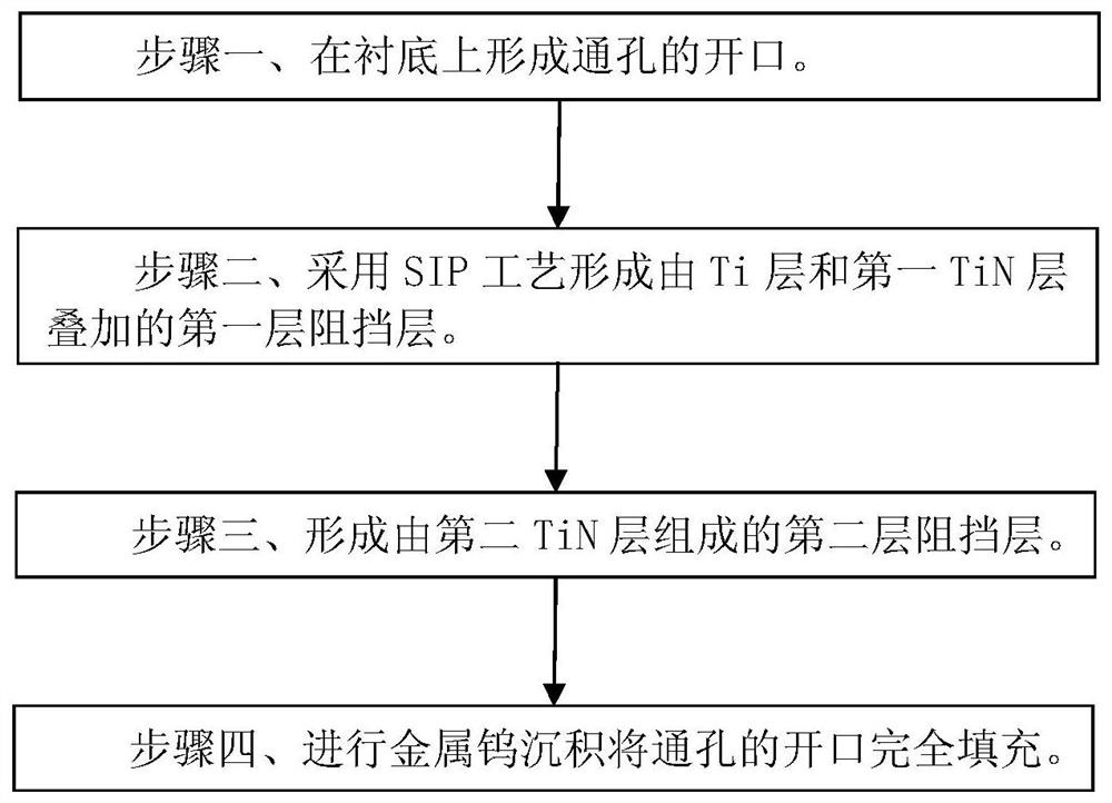
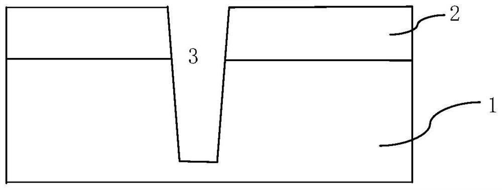
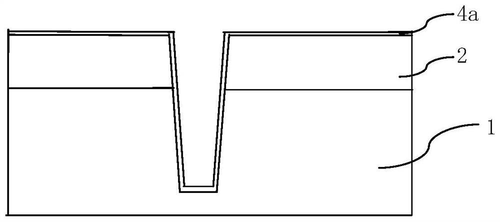
[0026] like figure 1 Shown is the flowchart of the manufacturing method of the through hole of the embodiment of the present invention, as Figure 2A to Figure 2C As shown, it is a schematic diagram of the device structure in each step of the method of the embodiment of the present invention. The method for manufacturing the through hole of the embodiment of the present invention includes the following steps:

[0027] Step 1, such as Figure 2A As shown, an opening 3 of a through hole is formed on a substrate 1 .

[0028] In the embodiment of the present invention, a bottom metal layer is formed on the substrate 1 in step 1, and an interlayer film 2 is formed on the bottom metal layer; the opening 3 of the through hole passes through the interlayer film 2. Figure 2A 2 only simply shows the structure of the interlayer film 2, the substrate 1 and the opening 3, and does not show the bottom metal layer. In practical applications, the bottom metal layer is located at the bott...


PUM

PropertyMeasurementUnit
thicknessaaaaaaaaaa
thicknessaaaaaaaaaa

Abstract

The invention discloses a manufacture method of a through hole. The method comprises the steps that 1 the opening of the through hole is formed in a substrate; 2 a SIP process is used to form a firstbarrier layer formed by superimposing a Ti layer and a first TiN layer; 3 a second barrier layer composed of a second TiN layer is formed; and 4 metal tungsten deposition is carried out to completelyfill the opening of the through hole. According to the invention, the film-forming quality of the barrier layers can be improved; tungsten residues are prevented; and the integrity of the product structure is improved.

Description

technical field [0001] The invention relates to a method for manufacturing a semiconductor integrated circuit, in particular to a method for manufacturing a through hole. Background technique [0002] In semiconductor devices, metal tungsten is generally used as a filling layer to connect the upper and lower metal layers, that is, in the through hole connecting the upper and lower metal layers, metal tungsten is usually used as a filling layer to fill the opening of the through hole, that is, Metal tungsten is used as the via hole. An interlayer film is usually formed between the upper and lower metal layers for isolation. The interlayer film is usually an oxide film, that is, a silicon dioxide film, that is, the sides of the through holes will be in contact with silicon dioxide; in order to prevent metal tungsten It reacts with the silicon dioxide at the bottom of the ground. Usually, before depositing metal tungsten, a barrier layer is deposited to prevent direct contact ...

Claims


Application Information

Patent Timeline
Patent Type & Authority Patents(China)
IPC IPC(8): H01L21/768
Inventor 刘善善朱兴旺朱黎敏
Owner SHANGHAI HUAHONG GRACE SEMICON MFG CORP
Why Eureka
Try Eureka