Manufacturing method for removing DBR film
A production method and film technology, which are applied in the field of DBR film removal, can solve the problems of high density, increase production time and cost, and difficult to remove DBR film, and achieve the effect of improving removal rate and facilitating removal.
- Summary
- Abstract
- Description
- Claims
- Application Information
AI Technical Summary
Problems solved by technology
Method used
Image

Examples
Embodiment 1
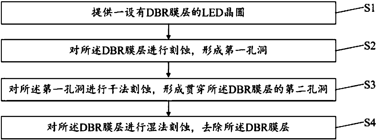
[0075] A method for removing a DBR film layer, comprising:
[0076] providing a sapphire substrate;
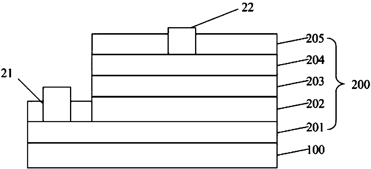
[0077] An epitaxial layer is formed on the sapphire substrate, and the epitaxial layer includes an N-type gallium nitride layer, an active layer and a P-type gallium nitride layer arranged on the surface of the sapphire substrate in sequence, and the thickness of the epitaxial layer is 6μm;
[0078] A transparent conductive layer doped with aluminum zinc oxide is formed on the surface of the P-type gallium nitride layer, and the thickness of the transparent conductive layer is
[0079] Etching the transparent conductive layer and the epitaxial layer to form a dicing line that penetrates the transparent conductive layer and extends to the first semiconductor layer;
[0080] forming a first electrode on the first semiconductor layer, and forming a second electrode on the transparent conductive layer;
[0081] forming a passivation layer on the surface of the transparent con...
Embodiment 2
[0088] A method for removing a DBR film layer, comprising:
[0089] providing a sapphire substrate;
[0090] An epitaxial layer is formed on the sapphire substrate, and the epitaxial layer includes an N-type gallium nitride layer, an active layer and a P-type gallium nitride layer arranged on the surface of the sapphire substrate in sequence, and the thickness of the epitaxial layer is 6μm;
[0091] A transparent conductive layer doped with aluminum zinc oxide is formed on the surface of the P-type gallium nitride layer, and the thickness of the transparent conductive layer is
[0092] Etching the transparent conductive layer and the epitaxial layer to form a dicing line that penetrates the transparent conductive layer and extends to the first semiconductor layer;
[0093] forming a first electrode on the first semiconductor layer, and forming a second electrode on the transparent conductive layer;
[0094] forming a passivation layer on the surface of the transparent con...
Embodiment 3
[0099] A method for removing a DBR film layer, comprising:
[0100] providing a sapphire substrate;
[0101] An epitaxial layer is formed on the sapphire substrate, and the epitaxial layer includes an N-type gallium nitride layer, an active layer and a P-type gallium nitride layer arranged on the surface of the sapphire substrate in sequence, and the thickness of the epitaxial layer is 6μm;
[0102] A transparent conductive layer doped with aluminum zinc oxide is formed on the surface of the P-type gallium nitride layer, and the thickness of the transparent conductive layer is
[0103] Etching the transparent conductive layer and the epitaxial layer to form a dicing line that penetrates the transparent conductive layer and extends to the first semiconductor layer;
[0104] forming a first electrode on the first semiconductor layer, and forming a second electrode on the transparent conductive layer;
[0105] forming a passivation layer on the surface of the transparent con...
PUM
| Property | Measurement | Unit |
|---|---|---|
| Diameter | aaaaa | aaaaa |
| Thickness | aaaaa | aaaaa |
| Thickness | aaaaa | aaaaa |
Abstract
Description
Claims
Application Information
 - R&D
- Intellectual Property
- Life Sciences
- Materials
- Tech Scout
- Unparalleled Data Quality
- Higher Quality Content
- 60% Fewer Hallucinations
Browse by: Latest US Patents, China's latest patents, Technical Efficacy Thesaurus, Application Domain, Technology Topic, Popular Technical Reports.
© 2025 PatSnap. All rights reserved.Legal|Privacy policy|Modern Slavery Act Transparency Statement|Sitemap|About US| Contact US: help@patsnap.com