Interconnection structure and manufacturing method thereof, and manufacturing method of semiconductor device

A manufacturing method and interconnection structure technology, which is applied in semiconductor/solid-state device manufacturing, electrical components, circuits, etc., can solve problems such as voids in the middle area, and achieve the effect of full filling of wiring materials and elimination of void defects

Active Publication Date: 2018-01-16
YANGTZE MEMORY TECH CO LTD
View PDF4 Cites 0 Cited by
  • Summary
  • Abstract
  • Description
  • Claims
  • Application Information

AI Technical Summary

Problems solved by technology

Due to the small width of the groove, when the interconnection line is made, it often occurs that when the groove is filled with wiring material, the opening area of ​​the groove is sealed by the wiring material, resulting in void defects in the middle area.

Method used


Image

  • Interconnection structure and manufacturing method thereof, and manufacturing method of semiconductor device
  • Interconnection structure and manufacturing method thereof, and manufacturing method of semiconductor device
  • Interconnection structure and manufacturing method thereof, and manufacturing method of semiconductor device

Examples


Embodiment Construction

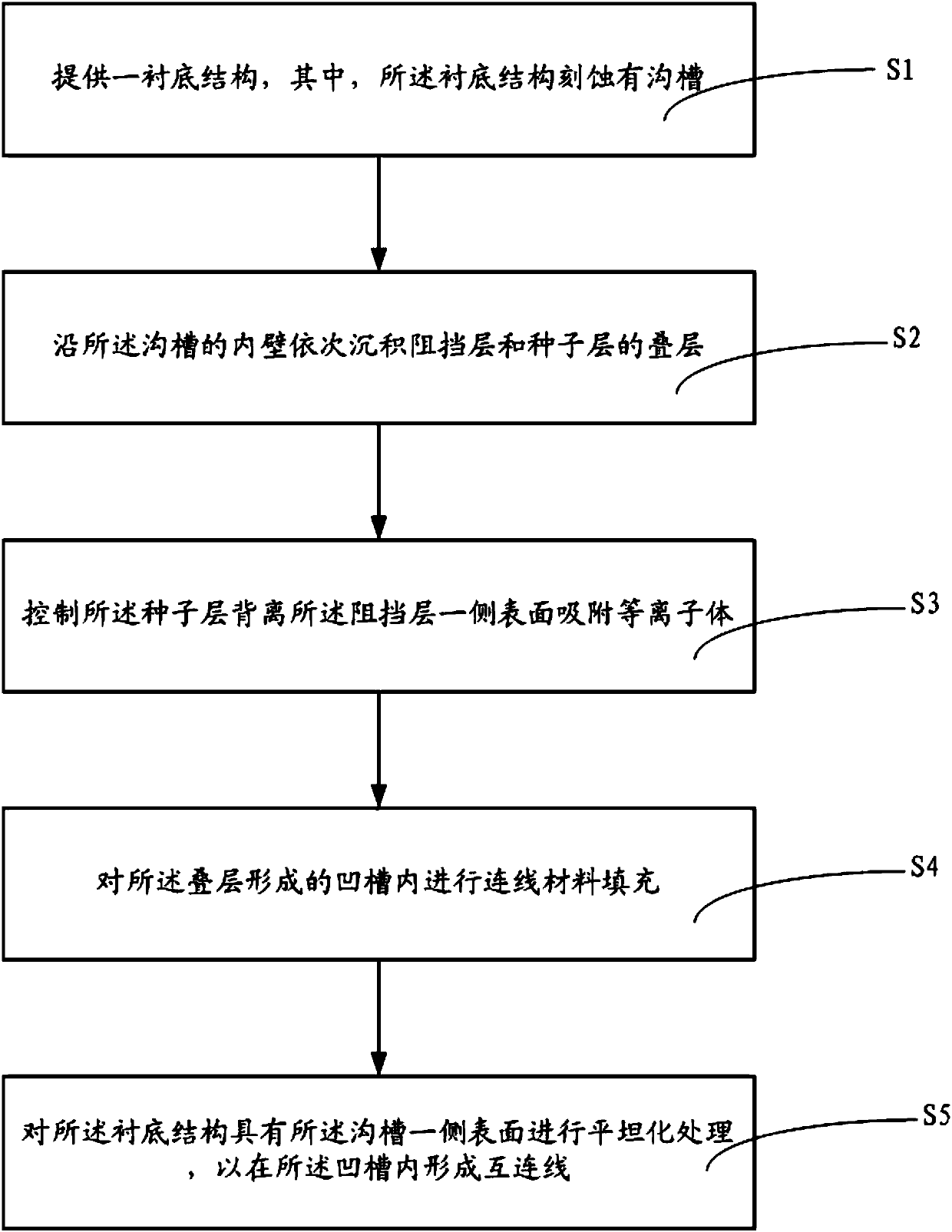
[0037] The following will clearly and completely describe the technical solutions in the embodiments of the present invention with reference to the accompanying drawings in the embodiments of the present invention. Obviously, the described embodiments are only some, not all, embodiments of the present invention. Based on the embodiments of the present invention, all other embodiments obtained by persons of ordinary skill in the art without making creative efforts belong to the protection scope of the present invention.

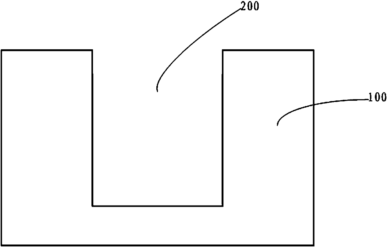
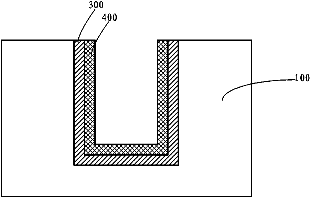
[0038] As described in the background, in the prior art, in the process of fabricating an interconnection structure, it is first necessary to fabricate a barrier layer and a seed layer stack in the trench, and then fabricate interconnection lines in the groove formed on the stack. Due to the small width of the groove, when the interconnection line is made, it often happens that when the groove is filled with the wiring material, the opening area of ​​the groove...


PUM

PropertyMeasurementUnit
Thicknessaaaaaaaaaa

Abstract

The invention discloses an interconnection structure and a manufacturing method thereof, and a manufacturing method of a semiconductor device. The manufacturing method of the interconnection structureincludes: providing a substrate structure, wherein a groove is etched in the substrate structure; depositing a lamination of a barrier layer and a seed layer in sequence along an inner wall of the groove; controlling the surface of one side of the seed layer, opposite to the barrier layer, to adsorb plasmas; filling the groove formed by the lamination with a connecting line material; and performing planarization processing on the surface of one side of the substrate structure, provided with the groove, to form interconnection lines in the groove. Before the filling of the connecting line material, the surface of one side of the seed layer, opposite to the barrier layer, adsorbs the plasmas; a region in which the plasmas are adsorbed on the surface of one side of the seed layer, opposite to the barrier layer, is optimized; the growing speed of the connecting line material in a region with small width of the groove is suppressed through the plasmas; the region with small width of the groove is prevented from being sealed; the filling of the connecting line material in the groove is fuller; and the defect of holes in the filling of the connecting line material is eliminated.

Description

technical field [0001] The invention relates to the technical field of interconnection structure fabrication, and more specifically, relates to an interconnection structure, a fabrication method thereof, and a fabrication method of a semiconductor device. Background technique [0002] At present, in the manufacturing process of semiconductor devices, multiple layers of metal interconnection layers can be formed on the substrate according to different needs, and each layer of metal interconnection layers includes interconnection lines, which requires trenching the dielectric layer on the substrate The etching of the interconnection line is then formed in the trench. The morphology and stability of the interconnection line have a great influence on the performance of the semiconductor device. In the prior art, in the process of fabricating an interconnection structure, it is first necessary to fabricate a stack of a barrier layer and a seed layer in a trench, and then fabricat...

Claims


Application Information

Patent Timeline
IPC IPC(8): H01L21/768
Inventor 彭浩万先进吴关平左明光周烽李远潘杰马亮
Owner YANGTZE MEMORY TECH CO LTD
Why Eureka
Try Eureka