
Ingan/alinn quantum well laser and manufacturing method thereof

A technology of lasers and quantum wells, applied in lasers, phonon exciters, laser components, etc., can solve the problem of increasing the threshold current of lasers and cavity surface scattering loss, reducing the radiative recombination of electrons and holes, and reducing the luminous efficiency of lasers and other problems to achieve the effect of weakening the polarization phenomenon, improving the polarization field, and increasing the internal quantum efficiency

Active Publication Date: 2019-11-05
SOUTH CHINA NORMAL UNIVERSITY
View PDF2 Cites 0 Cited by
  • Summary
  • Abstract
  • Description
  • Claims
  • Application Information

AI Technical Summary

Problems solved by technology

Traditional GaN-based quantum well lasers use InGaN as the well layer and GaN as the barrier layer. Due to the large lattice mismatch between the barrier and the well, it will lead to high defect density during the growth process, which will affect the quality of the laser.
Moreover, the existence of lattice mismatch will also cause a large polarization effect in the quantum well, reduce the radiative recombination of electrons and holes, and reduce the luminous efficiency of the laser.
In addition, studies have shown that GaN-based quantum well lasers usually use GaN as the waveguide layer, and the existence of a large lattice mismatch between the upper waveguide layer and the electron blocking layer increases the stress of the material, resulting in delamination of the laser cavity surface. , which increases the threshold current of the laser and the scattering loss of the cavity surface, which affects the far-field characteristics of the laser

Method used


Image

  • Ingan/alinn quantum well laser and manufacturing method thereof
  • Ingan/alinn quantum well laser and manufacturing method thereof
  • Ingan/alinn quantum well laser and manufacturing method thereof

Examples


Embodiment Construction

[0039] In order to make the object, technical solution and advantages of the present invention clearer, the present invention will be further described in detail below in conjunction with the accompanying drawings and specific implementation methods. It should be understood that the specific embodiments described here are only used to explain the present invention, and do not limit the protection scope of the present invention.

[0040] In terms of the present invention, p-type means doped with Mg, and n-type means doped with Si.

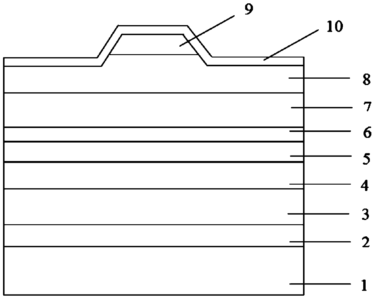
[0041] Such as figure 1 , an InGaN / AlInN quantum well laser, including from bottom to top: substrate 1, buffer layer 2, lower cladding layer 3, lower V-shaped waveguide layer 4, active region 5, electron blocking layer 6, upper V-shaped waveguide layer 7 , upper cladding layer 8 , ohmic contact layer 9 and electrodes 10 .

[0042] Further, in this embodiment, the substrate 1 is a GaN substrate, which is homoepitaxial.

[0043] Further, in this em...


PUM


Abstract

The invention discloses an InGaN / AlInN quantum well laser, comprising a substrate, a buffer layer, a lower covering layer, a lower V-shaped waveguide layer, an active region, an electronic blocking layer, an upper V-shaped waveguide layer, an upper covering layer, an ohmic contact layer and electrodes; both the upper V-shaped waveguide layer and the lower V-shaped waveguide layer are of AlGaN material, and the active region is an InGaN / AlInN quantum well layer. The InGaN / AlInN quantum well laser uses the AlGaN material as the waveguide layer and the active region, the AlInN material as a barrier layer and InGaN as a well layer, lattice mismatch of the materials is decreased, weak polarization occurs to the active region, polarization field and cavity face loss is low, threshold current islow, and the InGaN / AlInN quantum well laser has excellent optical properties.

Description

technical field [0001] The invention relates to the technical field of quantum well lasers, in particular, the invention relates to an InGaN / AlInN quantum well laser and a manufacturing method thereof. Background technique [0002] In recent years, III-V nitride materials have attracted much attention due to their large forbidden band width and wide tunable bandgap range. Common III-V nitrides such as GaN, AlN, and InN can form a continuous ternary alloy system with a direct bandgap width covering the wavelength range from infrared to ultraviolet. Quantum well laser is a kind of heterojunction laser with ultra-thin layer quantum well structure as the active region. Compared with gas lasers and solid-state lasers, quantum well lasers can freely choose the appropriate material and thickness of the active region, and have a wide range of emission wavelengths and high photoelectric conversion efficiency. Applying III-V nitride materials to quantum well lasers can improve the p...

Claims


Application Information

Patent Timeline
Patent Type & Authority Patents(China)
IPC IPC(8): H01S5/343
Inventor 郭志友侯玉菲孙慧卿汪鑫张秀龚星徐智鸿刘天意
Owner SOUTH CHINA NORMAL UNIVERSITY
Learn More