Flexible organic light-emitting diode (OLED) display panel

A display panel, flexible technology, used in instruments, electrical components, electrical solid devices, etc., can solve the problems of easy cracking, unfavorable dispersion of mechanical stress, low elasticity of inorganic layers, etc., to increase flexibility and flexibility, ensure Water and oxygen barrier performance and the effect of improving reliability

Active Publication Date: 2018-01-05
WUHAN CHINA STAR OPTOELECTRONICS SEMICON DISPLAY TECH CO LTD
View PDF4 Cites 13 Cited by
  • Summary
  • Abstract
  • Description
  • Claims
  • Application Information

AI Technical Summary

Problems solved by technology

However, there is a disadvantage when adopting the whole-surface organic layer and inorganic layer multi-layer barrier structure packaging, that is, the inorganic layer has low elasticity, which is not conducive to dispersing mechanical stress. The risk of cracking is prone to occur during the process, which will cause water and oxygen to enter the device through the cracks, causing the failure of the OLED display panel
[0004] To sum up, the flexible OLED display panel in the prior art is encapsulated by a whole layer of thin film encapsulation layer composed of inorganic thin film and organic thin film. Due to the low elasticity of the inorganic layer, it is not conducive to dispersing mechanical stress. Cracks are prone to occur in the process of curling or folding, which will cause water and oxygen to enter the device through the cracks, which will cause the failure of the OLED device

Method used


Image

  • Flexible organic light-emitting diode (OLED) display panel
  • Flexible organic light-emitting diode (OLED) display panel
  • Flexible organic light-emitting diode (OLED) display panel

Examples


Embodiment Construction

[0029] The following descriptions of the various embodiments refer to the accompanying drawings to illustrate specific embodiments in which the invention may be practiced. The directional terms mentioned in the present invention, such as [top], [bottom], [front], [back], [left], [right], [inside], [outside], [side], etc., are only for reference The orientation of the attached schema. Therefore, the directional terms used are used to illustrate and understand the present invention, but not to limit the present invention. In the figures, structurally similar elements are denoted by the same reference numerals.

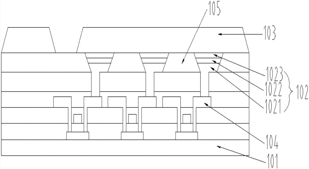
[0030] The present invention aims at the existing flexible OLED display panel, solves the flexible OLED display panel of the prior art, and encapsulates it with a thin film encapsulation layer composed of an inorganic thin film and an organic thin film. Because the elasticity of the inorganic layer is low, it is not conducive to To disperse mechanical stress, it is eas...


PUM


Abstract

The invention provides a flexible organic light-emitting diode (OLED) display panel. The flexible OLED display panel comprises a flexible substrate, an OLED device and a thin film encapsulation layer,wherein the OLED device is arranged on the substrate, the thin film encapsulation layer is arranged on a surface of the OLED device and at least comprises two thin film encapsulation units independent to each other, the at least two thin film encapsulation units cover a surface, deviating from the flexible substrate, of the OLED device in a mode of one-dimensional array or two-dimensional array,and a gap is formed between edges of adjacent two thin film encapsulation units. By the flexible OLED display panel, the technical problem that the flexible OLED display panel of the prior part is easy to crack during bending by encapsulation of the whole thin film encapsulation layer to cause that water and oxygen enter the device through cracks to further cause failure of the OLED device is solved.

Description

technical field [0001] The invention relates to the technical field of flexible display, in particular to a flexible OLED display panel. Background technique [0002] Organic Light-Emitting Diode (OLED) display device has all solid-state, self-luminous, no backlight, low driving voltage, low energy consumption, fast response, wide operating temperature range, high luminous efficiency, wide viewing angle, With the advantages of thinness and flexible display, it has become the most promising new display device in recent years. [0003] Among them, the use of flexible substrates to make bendable flexible displays is an important development direction of OLEDs. Since the electrode materials and luminescent materials of the OLED device are sensitive to oxygen and water vapor, the OLED device will fail. Therefore, effective encapsulation of the OLED display device, so that each functional layer of the OLED device is fully separated from components such as water vapor and oxygen ...

Claims


Application Information

Patent Timeline
Patent Type & Authority Applications(China)
IPC IPC(8): H01L27/32H01L51/52H01L51/56G09F9/30
CPCG09F9/30H10K59/00H10K50/80H10K71/00
Inventor 陈哲
Owner WUHAN CHINA STAR OPTOELECTRONICS SEMICON DISPLAY TECH CO LTD
Why Eureka
Try Eureka