Manufacturing method of semiconductor device

A manufacturing method and semiconductor technology, applied in semiconductor devices, semiconductor/solid-state device manufacturing, electrical components, etc., can solve problems such as gate oxide layer breakdown damage, achieve the effect of avoiding breakdown damage and ensuring overall performance

Active Publication Date: 2017-12-19
FOUNDER MICROELECTRONICS INT
View PDF4 Cites 2 Cited by
  • Summary
  • Abstract
  • Description
  • Claims
  • Application Information

AI Technical Summary

Problems solved by technology

[0011] The invention provides a method for manufacturing a semiconductor device to solve the problem in the prior art that when the gate is formed by dry etching, it is easy to cause breakdown damage to the gate oxide layer

Method used


Image

  • Manufacturing method of semiconductor device
  • Manufacturing method of semiconductor device
  • Manufacturing method of semiconductor device

Examples


Embodiment 1

[0038] This embodiment provides a method for manufacturing a semiconductor device, which is used for manufacturing a semiconductor device.

[0039] Such as figure 2 Shown is a schematic flow chart of the manufacturing method of the semiconductor device according to this embodiment. The manufacturing method of the semiconductor device includes:

[0040] Step 201, forming a gate oxide layer on a semiconductor substrate.

[0041] The semiconductor substrate in this embodiment can be a silicon substrate, a sapphire substrate, or any other semiconductor substrate, which can be selected according to actual needs.

[0042] The gate oxide layer in this embodiment may be silicon dioxide. For example, if the semiconductor substrate is a silicon substrate, the gate oxide layer may be formed by oxidizing the silicon substrate. The growth temperature of the gate oxide layer is 900° C. to 1200° C. ℃, the thickness is 0.01 micron to 1.0 micron.

[0043] Step 202, forming a gate material...

Embodiment 2

[0053] In this embodiment, a further supplementary description is given to the manufacturing method of the semiconductor device in the first embodiment.

[0054] Such as Figures 3A to 3F Shown is a schematic structural view of each step of the manufacturing method of the semiconductor device according to this embodiment.

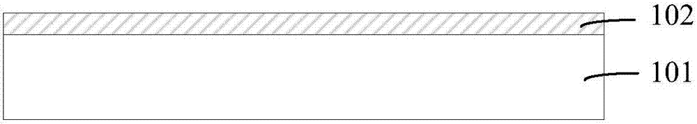
[0055] Such as Figure 3A As shown, a gate oxide layer 302 is formed on a semiconductor substrate 301 .

[0056] The semiconductor substrate 301 in this embodiment may be a silicon substrate, a sapphire substrate, or any other semiconductor substrate, which may be selected according to actual needs.

[0057] The gate oxide layer 302 in this embodiment may be silicon dioxide. For example, if the semiconductor substrate 301 is a silicon substrate, the gate oxide layer may be formed by oxidizing the silicon substrate. The growth temperature of the gate oxide layer 302 is 900° C.˜1200° C., and the thickness is 0.01 μm˜1.0 μm.

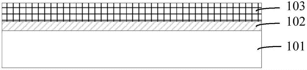
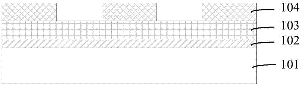
[0058] Such as Figure 3B As s...


PUM

PropertyMeasurementUnit
thicknessaaaaaaaaaa
temperatureaaaaaaaaaa
thicknessaaaaaaaaaa

Abstract

The invention provides a manufacturing method of a semiconductor device. The method comprises the following steps of forming a grid oxide layer on a semiconductor base; forming a grid material layer on the grid oxide layer; and using a dry method etching technology to etch the grid material layer so as to form a grid electrode and carrying out deion processing on the grid material layer during a grid electrode formation process. In the invention, during a process of using the dry method etching technology to etch the grid material layer so as to form the grid electrode, deion processing is performed on the grid material layer so that conditions that excess ions are accumulated in the grid material layer and the grid oxide layer generates breakdown damages are avoided, and then integral performance of the semiconductor device can be guaranteed.

Description

technical field [0001] The invention relates to semiconductor technology, in particular to a manufacturing method of a semiconductor device. Background technique [0002] A semiconductor refers to a material whose conductivity is between that of a conductor and an insulator at room temperature. The conductivity of semiconductors is controllable, ranging from insulators to a few ohms. Nowadays, the core units of most electronic products, such as computers, mobile phones or tape recorders, are closely related to semiconductors, which are widely used in various electronic devices. [0003] The methods of making semiconductors in the prior art are as follows: [0004] Such as Figure 1A As shown, a gate oxide layer 102 is formed on a semiconductor substrate 101 . [0005] The semiconductor substrate 101 may be a silicon substrate. [0006] Such as Figure 1B As shown, a gate material layer 103 is formed on the gate oxide layer 102 . [0007] The material of the gate materi...

Claims


Application Information

Patent Timeline
Patent Type & Authority Applications(China)
IPC IPC(8): H01L21/28H01L21/3213
CPCH01L21/28026H01L21/28247H01L21/32135H01L21/32138
Inventor 马万里赵圣哲
Owner FOUNDER MICROELECTRONICS INT
Why Eureka
Try Eureka