Image module structure

An image module and image sensor technology, which is applied in image communication, television, color television, etc., can solve the problems of optical axis offset, unsuitable for miniaturized devices, and optical axis alignment, etc., so as to improve quality and improve The effect of difficult alignment and easy alignment

Inactive Publication Date: 2017-11-17
FUGANG ELECTRONICS DONGGUAN +1
View PDF3 Cites 2 Cited by
  • Summary
  • Abstract
  • Description
  • Claims
  • Application Information

AI Technical Summary

Problems solved by technology

However, the thickness of such a module structure has tended to be stable, and it is not suitable for putting into today's miniaturized devices, especially the circuit board 1500 is usually a composite material. During the process of circuit board processing, due to thermal stress, chemical factors or It is an improper production process that causes warpage on the circuit board. If the image sensor or substrate is placed on the circuit board, it will cause problems with optical axis alignment, and even cause optical axis deviation, especially for multiple images. Sensors require precise optical axis alignment. Therefore, it is necessary to develop a module structure that can accurately align the optical axes of multiple image sensors.

Method used


Image

  • Image module structure
  • Image module structure
  • Image module structure

Examples


Embodiment Construction

[0019] In order to describe the technical content, structural features, purpose and effect of the present invention in detail, the following examples are given together with the drawings to describe in detail.

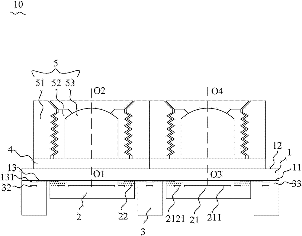
[0020] see figure 2 as shown, figure 2 As an embodiment of the present invention, an image module structure 10 includes a glass substrate 1 , a plurality of image sensors 2 , a circuit board 3 , a carrier pad 4 , and a lens device 5 .

[0021] In this embodiment, the design of two lens devices 5 is used as a schematic diagram of the present invention. Wherein, the glass substrate 1 has a first surface 11 and a second surface 12 , and a plurality of image sensors 2 are disposed on the first surface 11 . The circuit board 3 is also arranged on the first surface 11, and has a plurality of hollow blocks 31 and a conductive area 32. The conductive area 32 is adjacent to the hollow blocks 31 and faces the glass substrate 1. Each hollow block 31 Corresponding to the posi...


PUM


Abstract

The present invention discloses an image module structure. The structure comprises a glass substrate, at least one image sensor, a circuit board and at least one lens device. The glass substrate comprises a first surface and a second surface which are oppositely arranged, the at least one image sensor is pasted on the first surface, the circuit board is connected with the first surface, at least one hollow block is formed on the circuit board, the at least one hollow block can hold the at least one image sensor, and the lens device is arranged at the second surface. The upper surface and the lower surface of the glass substrate are flat and parallel, and the at least one image sensor and the lens device are arranged on the glass substrate so as to improve the problem that the contraposition of an optical axis is not easy, improve the imaging quality and reduce the whole structure height through the technical means of the at least one hollow blocks in the circuit board.

Description

technical field [0001] The invention relates to an image module structure, in particular to an image module structure with a plurality of image sensors. Background technique [0002] Most of the modern electronic components are developed in the direction of thinning and multi-functional integration. How to design more user-friendly products with multi-unit functions is one of the main research and development topics of various manufacturers. [0003] In recent years, with the miniaturization of imaging devices such as photosensitive coupling devices (CCD, Charge Coupled Device) and complementary metal oxide semiconductors (CMOS, Complementary Metal-Oxide Semiconductor), the CCD type image sensor or CMOS type Image sensors are gradually widely used in digital products, such as smart phones, tablet computers, notebook computers, driving recorders, etc. Among them, the smart phones that are closest to people's lives are the most competitive, and the photos taken by the camera d...

Claims


Application Information

Patent Timeline
Patent Type & Authority Applications(China)
IPC IPC(8): H04N5/225H04N5/335H01L27/146H04N25/00
CPCH01L27/14601H01L27/14618H04N23/54H04N23/55H04N25/00
Inventor 罗瑞祥施玉庭
Owner FUGANG ELECTRONICS DONGGUAN
Why Eureka
Try Eureka