Power protection device and circuit board testing system

A protective device and circuit board technology, applied in the direction of electronic circuit testing, measuring devices, measuring electricity, etc., can solve problems such as damage to electronic components, achieve the effects of reducing losses, improving product yield, and avoiding damage

Inactive Publication Date: 2017-11-17
XIAN YIPU COMM TECH
View PDF6 Cites 2 Cited by
  • Summary
  • Abstract
  • Description
  • Claims
  • Application Information

AI Technical Summary

Problems solved by technology

However, the inventor finds that there are following problems in the prior art: the circuit board to be tested is protected by using TVS diodes, such as Figure 1A Shown is a schematic diagram of the waveform of the first input voltage (that is, the waveform of the output voltage at the power supply terminal), as shown in Figure 1B Shown is the schematic diagram of the waveform of th...

Method used


Image

  • Power protection device and circuit board testing system
  • Power protection device and circuit board testing system
  • Power protection device and circuit board testing system

Examples


Embodiment Construction

[0026] In order to make the object, technical solution and advantages of the present invention clearer, various embodiments of the present invention will be described in detail below in conjunction with the accompanying drawings. However, those of ordinary skill in the art can understand that, in each implementation manner of the present invention, many technical details are provided for readers to better understand the present application. However, even without these technical details and various changes and modifications based on the following implementation modes, the technical solution claimed in this application can also be realized.

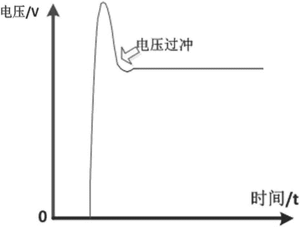
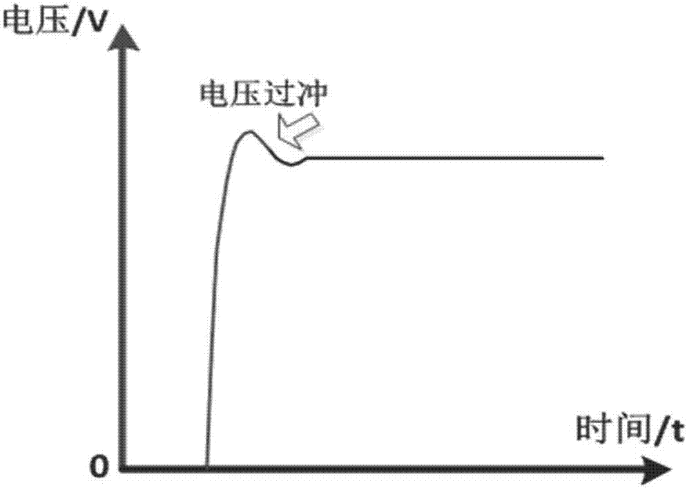
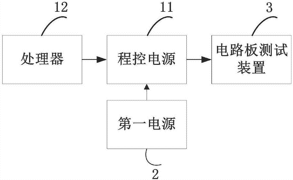
[0027] The first embodiment of the present invention relates to a power protection device, the power protection device includes at least one programmable power supply 11 and a processor 12, such as figure 2 Shown (take a program-controlled power supply as an example).

[0028] In this embodiment, the control terminal of the programmable p...


PUM


Abstract

Embodiments of the invention relate to the technical field of electronic products, and disclose a power protection device and a circuit board testing system. In the embodiments of the invention, the power protection device includes at least one programmable power supply and a processor; a control end of the programmable power supply is connected with the processor, a voltage input end of the programmable power supply is configured to connect to a first power supply, and a voltage output end of the programmable power supply is configured to connect to a circuit board testing device; and the processor is configured to control the programmable power supply to convert the voltage output by the first power supply into a step voltage and supply power to the circuit board testing device. The embodiments of the invention further provide the circuit board testing system. The embodiments of the invention solve the voltage overshoot problem caused by instantly turning on the power supply, avoid the damage to electronic components on a circuit board, improve the product yield and reduce the loss.

Description

technical field [0001] The embodiments of the present invention relate to the technical field of electronic products, in particular to a power supply protection device and a circuit board testing system. Background technique [0002] Electrical Over Stress (EOS) shock means that when the current or voltage applied to an electronic component exceeds the maximum design specification requirements that the electronic component can withstand, the performance of the electronic component will be weakened or even directly damaged. The phenomenon. For example, when the circuit board test device tests the circuit board to be tested, if the voltage of the circuit board to be tested exceeds its maximum withstand value, the function of the electronic components installed on the circuit board to be tested will be weakened or damaged, especially for the power supply environment. In places (such as factories), the probability of EOS impact is relatively high; therefore, how to reduce the E...

Claims


Application Information

Patent Timeline
IPC IPC(8): G01R31/28
CPCG01R31/2818
Inventor 乔洋
Owner XIAN YIPU COMM TECH
Why Eureka
Try Eureka