Bonding heating control device and method thereof

A heating control device and heating device technology, which are applied in the manufacture of semiconductor/solid state devices, semiconductor devices, electrical components, etc., can solve the problems of unstable heating, excessive heating time, and vibration of heating temperature, and achieve the effect of reducing oscillation, The effect of improving the heating effect and improving the productivity

Active Publication Date: 2020-05-01
SHANGHAI MICRO ELECTRONICS EQUIP (GRP) CO LTD
View PDF8 Cites 0 Cited by
  • Summary
  • Abstract
  • Description
  • Claims
  • Application Information

AI Technical Summary

Problems solved by technology

[0006] The purpose of the present invention is to provide a bonding heating control device and its method, which can solve the problems in the prior art that the heating time is too long, the heating is unstable, and the heating temperature oscillates

Method used


Image

  • Bonding heating control device and method thereof
  • Bonding heating control device and method thereof
  • Bonding heating control device and method thereof

Examples


Embodiment Construction

[0034] In order to make the content of the present invention clearer and easier to understand, the content of the present invention will be further described below in conjunction with the accompanying drawings. Of course, the present invention is not limited to this specific embodiment, and general replacements known to those skilled in the art are also covered within the protection scope of the present invention.

[0035] Secondly, the present invention is described in detail by means of schematic diagrams. When describing the examples of the present invention in detail, for the convenience of illustration, the schematic diagrams are not partially enlarged according to the general scale, which should not be used as a limitation of the present invention.
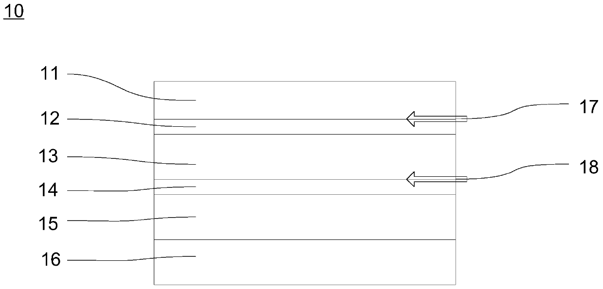
[0036] The core idea of ​​the present invention is: measure the temperature of each temperature sensor in the two heating devices by the heating controller, respectively output the PWM opening degrees of the heaters in the tw...


PUM


Abstract

The invention provides a bonding heating control device and a method thereof. The device comprises a heating controller, two heating devices and two heating driving devices. Each heating device is used for heating and pressurizing a silicon wafer or a glass sheet. Each heating device is provided with a heater and at least two temperature sensors. The heating controller is used for measuring each temperature sensor in the two heating devices and outputting PWM opening of a heater. Each heating driving device drives the heater to work according to the PWM opening output by the heating controller. The two heating devices work independently at the same time so that heating time is saved and heating efficiency is improved. Graphite pieces are arranged on upper and lower sides of a heating disc so as to make the temperature spread evenly. Meanwhile, a heating process is divided into three stages, rapid heating in a rate heating stage shortens the heating time and increases a yield; and adjustable power in a heating rate stage is realized and more process parameters are provided for a bonding process.

Description

technical field [0001] The invention relates to the technical field of semiconductors, in particular to a bonding heating control device and a method thereof. Background technique [0002] Two wafers with flat and clean surfaces can be bonded to each other through chemical bonds on the surface under certain conditions, without being limited by the crystal lattice and crystal orientation of the two wafer materials. This technology is called wafer bonding technology. . Using bonding technology to combine new structural materials has a great degree of freedom, so it is widely used in microelectronic circuits, sensors, power devices, micromachining, optoelectronic devices, silicon-on-insulator wafers (SOI) and other fields. Wafer bonding technology has become a technology that can be used to fabricate many important optoelectronic devices. [0003] Wafer bonding technology can bond wafers of different materials together. Wafer bonding is an important process for three-dimensi...

Claims


Application Information

Patent Timeline
Patent Type & Authority Patents(China)
IPC IPC(8): H01L21/67H01L21/60
CPCH01L21/67098H01L24/03
Inventor 罗晋商飞祥
Owner SHANGHAI MICRO ELECTRONICS EQUIP (GRP) CO LTD
Why Eureka
Try Eureka