Negative Voltage Comparator Circuit
A voltage comparator and comparator technology, applied in the direction of instruments, electric variable adjustment, control/regulation systems, etc., can solve problems such as unfavorable production, failure to provide negative power supply and negative reference source, and heavy adjustment workload, etc., to achieve Effects of easy to implement, low cost, high precision negative voltage comparison
- Summary
- Abstract
- Description
- Claims
- Application Information
AI Technical Summary
Problems solved by technology
Method used
Image
Examples
Embodiment 1
[0025] The invention proposes a new type of comparison circuit, which can still realize negative voltage comparison without using negative electricity and negative reference source, and has high judgment accuracy.
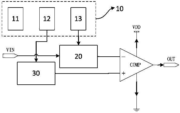
[0026] Such as figure 1 As shown, it specifically includes a comparator COMP, a current mirror 10 , an input signal circuit 20 and a reference signal circuit 30 .
[0027] Wherein, the input signal circuit 20 is used for receiving the voltage signal to be compared. The reference signal circuit 30 is used to input a reference signal to the comparator COMP. In order to improve and ensure higher comparison accuracy, the current mirror 10 provides equal bias currents for the input signal circuit 20 and the reference signal circuit 30 , so that the electrical environment is the same. Since the present invention is used for comparison of negative voltages, the input signal circuit 20 is connected to the negative input terminal of the comparator COMP, and the reference ...
Embodiment 2
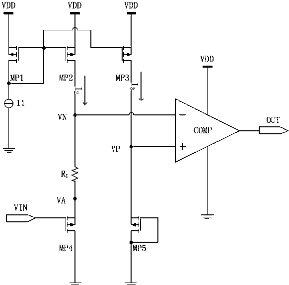
[0031] As a further optimization of Embodiment 1, the difference between this embodiment and Embodiment 1 is that, as figure 2 As shown, in this embodiment, the current mirror 10 is composed of three mirror circuits including MOS transistors, wherein the first mirror circuit 11 includes a first MOS transistor MP1 and a current source, the source of the first MOS transistor MP1 is connected to a power supply, and the gate The pole and the drain are connected to ground through a current source. The second mirror circuit 12 includes a second MOS transistor MP2. The source of the second MOS transistor MP2 is connected to the power supply, the gate is connected to the first mirror circuit 11 , and the drain is connected to the input signal circuit 20 . The third mirror circuit 13 includes a third MOS transistor MP3 , the source of the third MOS transistor MP3 is connected to the power supply, the gate is connected to the first mirror circuit 11 , and the drain is connected to the ...
PUM
 Abstract
Description
Claims
Application Information
 - R&D
- Intellectual Property
- Life Sciences
- Materials
- Tech Scout
- Unparalleled Data Quality
- Higher Quality Content
- 60% Fewer Hallucinations
Browse by: Latest US Patents, China's latest patents, Technical Efficacy Thesaurus, Application Domain, Technology Topic, Popular Technical Reports.
© 2025 PatSnap. All rights reserved.Legal|Privacy policy|Modern Slavery Act Transparency Statement|Sitemap|About US| Contact US: help@patsnap.com


