Display panel and display device

A display panel and substrate technology, which is applied to circuit devices, printed circuit grounding devices, instruments, etc., can solve the problems of unfavorable narrow frame of display panel and enlargement of lower frame area, so as to achieve narrow frame, reduce area, The effect of preventing static electricity

Active Publication Date: 2017-10-13
XIAMEN TIANMA MICRO ELECTRONICS
View PDF4 Cites 33 Cited by
  • Summary
  • Abstract
  • Description
  • Claims
  • Application Information

AI Technical Summary

Problems solved by technology

[0004] However, with the development of display technology, the resolution of the display panel is getting higher and higher, and more wiring (such as data wiring for transmitting data signals) needs to be arranged in the frame area (especially the lower frame area), and the ground welding The setting of the panel will also occupy part of the lower frame area, which will cause the lower frame area (also called the step area) to become larger, which is not conducive to the narrower frame of the display panel.

Method used


Image

  • Display panel and display device
  • Display panel and display device
  • Display panel and display device

Examples


Embodiment Construction

[0023] The application will be further described in detail below in conjunction with the accompanying drawings and embodiments. It should be understood that the specific embodiments described here are only used to explain related inventions, rather than to limit the invention. It should also be noted that, for ease of description, only parts related to the invention are shown in the drawings.

[0024] It should be noted that, in the case of no conflict, the embodiments in the present application and the features in the embodiments can be combined with each other. The present application will be described in detail below with reference to the accompanying drawings and embodiments.

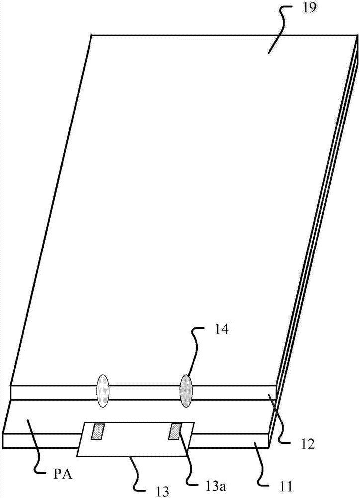
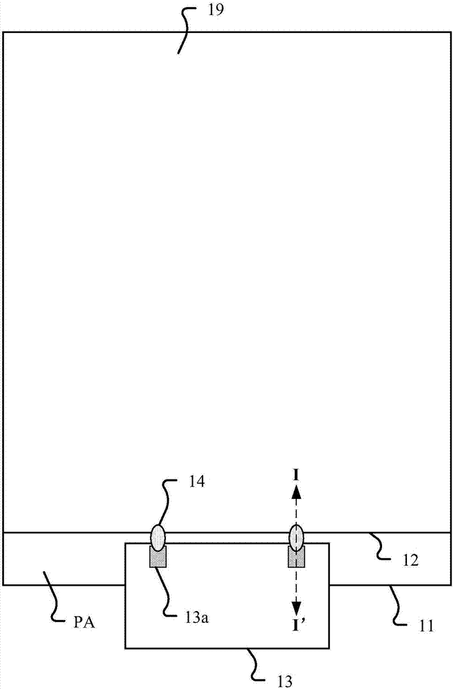
[0025] figure 1 A schematic diagram of a display panel according to an embodiment of the present application is shown.

[0026] Such as figure 1 As shown, the display panel may include a conductive adhesive 14 , a chip-on-chip film 13 , a conductive layer 19 , and a first substrate 11 and a seco...


PUM


Abstract

The invention discloses a display panel and a display device, and belongs to the field of display technologies. The display panel comprises electrically conductive adhesion bodies, a chip on film, an electrically conductive layer, a first substrate and a second substrate. The first substrate is opposite to the second substrate, the chip on film is adhered at a step region of the first substrate, and the electrically conductive layer is positioned on the side, which is far away from the first substrate, of the second substrate; the chip on film comprises a grounding bonding pad, and the grounding bonding pad is arranged on the side, which is far away from the first substrate, of the chip on film; the electrically conductive adhesion bodies are electrically connected with the electrically conductive layer and are electrically connected with the grounding bonding pad. According to the technical scheme, the display panel and the display device have the advantages that the grounding bonding pad is arranged on the side, which is far away from the first substrate, of the chip on film, accordingly, the occupied area of the step regions can be reduced while static electricity is prevented, and frames of the display panel can be advantageously narrowed.

Description

technical field [0001] The present application relates to the field of display technology, in particular to a display panel and a display device. Background technique [0002] Liquid crystal displays have the advantages of low radiation, small size, and low energy consumption. They have gradually replaced traditional cathode ray tube displays and are widely used in flat-screen TVs, personal computers, and other portable products. [0003] A liquid crystal display panel in the prior art generally includes an array substrate, a color filter substrate, and a liquid crystal layer disposed between the array substrate and the color filter substrate. Since the display panel will generate static electricity on the color filter substrate during use, it is necessary to arrange a layer of antistatic film on the color filter substrate, and connect the antistatic film to the grounding pad provided on the array substrate, so that the Electrostatic conduction on the color filter substrate...

Claims


Application Information

Patent Timeline
Patent Type & Authority Applications(China)
IPC IPC(8): G02F1/1345
CPCG02F1/13458H05K1/0215H05K3/321H05K2201/09409H05K2201/09845G02F1/13452H05K3/323H05K2201/09781G02F1/133305H01L23/49572H01L23/49838H01L23/4985H01L23/49855H01L23/5387H01L23/5388H01L23/562H01L24/50H01L24/81H05K1/0271H05K1/0393H05K1/118H05K1/188H05K1/189H05K3/0097H05K2201/2009
Inventor 赖国昌周洪波
Owner XIAMEN TIANMA MICRO ELECTRONICS
Why Eureka
Try Eureka