
Method for manufacturing connector

A manufacturing method and connecting body technology, applied in semiconductor/solid-state device manufacturing, printed circuit manufacturing, equipment for manufacturing conductive/semiconductive layers, etc., can solve problems such as alignment deviation, narrowing of spacing, short-circuit connection, etc., Achieve the effect of preventing misalignment and suppressing poor connection

Active Publication Date: 2017-10-03
DEXERIALS CORP
View PDF6 Cites 0 Cited by
  • Summary
  • Abstract
  • Description
  • Claims
  • Application Information

AI Technical Summary

Problems solved by technology

Due to this misalignment, the distance between the electrode terminal of the liquid crystal driving IC and the terminal portion adjacent to the terminal portion of the transparent substrate connected to the electrode terminal will be narrowed. Tendency to poor connections such as short circuits
In addition, this misalignment may occur when electronic components are mounted

Method used


Image

  • Method for manufacturing connector
  • Method for manufacturing connector
  • Method for manufacturing connector

Examples


Embodiment 1

[0075] An anisotropic conductive film was arranged on the evaluation substrate, and an IC for evaluation was arranged on the evaluation substrate through the anisotropic conductive film. Using an ultraviolet irradiator (ZUV-C30H: manufactured by Omron Corporation), ultraviolet rays were irradiated from the disposed evaluation IC side (step (C)), and provisional crimping was performed. After provisional crimping, from the IC side for evaluation, thermal pressurization was performed with a thermocompression bonding tool, and ultraviolet rays were irradiated with an ultraviolet irradiator (step (D)), and main crimping was performed to obtain a connected body sample.

[0076] The amount of ultraviolet radiation during temporary crimping is set to 200mJ / cm 2 . In addition, the actual pressure bonding conditions were 100° C., 80 MPa, and 5 seconds. When pressing, a Teflon (registered trademark) sheet with a thickness of 50 μm was used as a buffer between the thermocompression bondi...

Embodiment 2

[0080] Changed the amount of UV irradiation during temporary crimping to 600mJ / cm 2 , except that, a linker sample was obtained under the same conditions as in Example 1.

Embodiment 3

[0082] Connected body samples were obtained under the same conditions as in Example 1, except that the ultraviolet illuminance and irradiation time during provisional crimping were changed, and only thermal pressing was performed during main crimping without ultraviolet irradiation.


PUM


Abstract

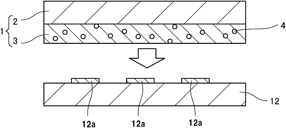
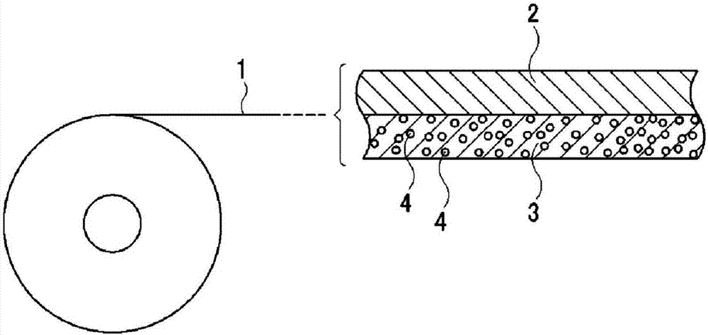
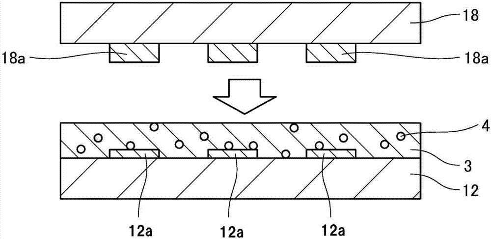
The invention relates to a method for manufacturing a connector. The object is to prevent an electrical component from alignment deviation in a connection procedure so as to prevent bad connector connection. The invention relates to a method for manufacturing a connector, and the method comprises the procedure (A) of configuring a photocurable anisotropic conductive film (1) on a first electronic component (12); the procedure (B) of configuring a second electronic component (18) on the first electronic component (12) separated by the anisotropic conductive film (1); the procedure (C) of illuminating from the second electronic component (18) side; and the procedure (D) of connecting the first electronic component (12) with the second electronic component (18) at the second electronic component (18) side using a heater.

Description

technical field [0001] The present invention relates to a method for producing a connection body in which a second electronic component is connected to a first electronic component through a photocurable anisotropic conductive film. Background technique [0002] Conventionally, liquid crystal display devices have been widely used as various display devices such as televisions, PC monitors, mobile phones, portable game machines, tablet PCs, and vehicle monitors. In recent years, the so-called COG (chip bonded on glass, chip bonded on glass) in which the liquid crystal driving IC is directly mounted on the substrate of the liquid crystal display panel has been adopted in such a liquid crystal display device from the viewpoint of finer pitch, lighter weight and thinner. chip on glass), so-called FOG (film on glass) in which a flexible substrate formed with a liquid crystal driving circuit is directly mounted on the substrate of a liquid crystal display panel (for example, refer...

Claims


Application Information

Patent Timeline
IPC IPC(8): H01L21/603
CPCH01L24/83H01L2224/83203H01L2224/83143H01L2224/83048H01L2224/73204H05K3/323H01B13/0026H05K2201/0108
Inventor 梶谷太一郎
Owner DEXERIALS CORP
Learn More