A signal processing circuit
A signal processing circuit and circuit technology, applied in the computer field, can solve problems such as the inability to flexibly control the working state of the resistive variable memory, and achieve the effect of a simple circuit structure
- Summary
- Abstract
- Description
- Claims
- Application Information
AI Technical Summary
Problems solved by technology
Method used
Image
Examples
Embodiment 1
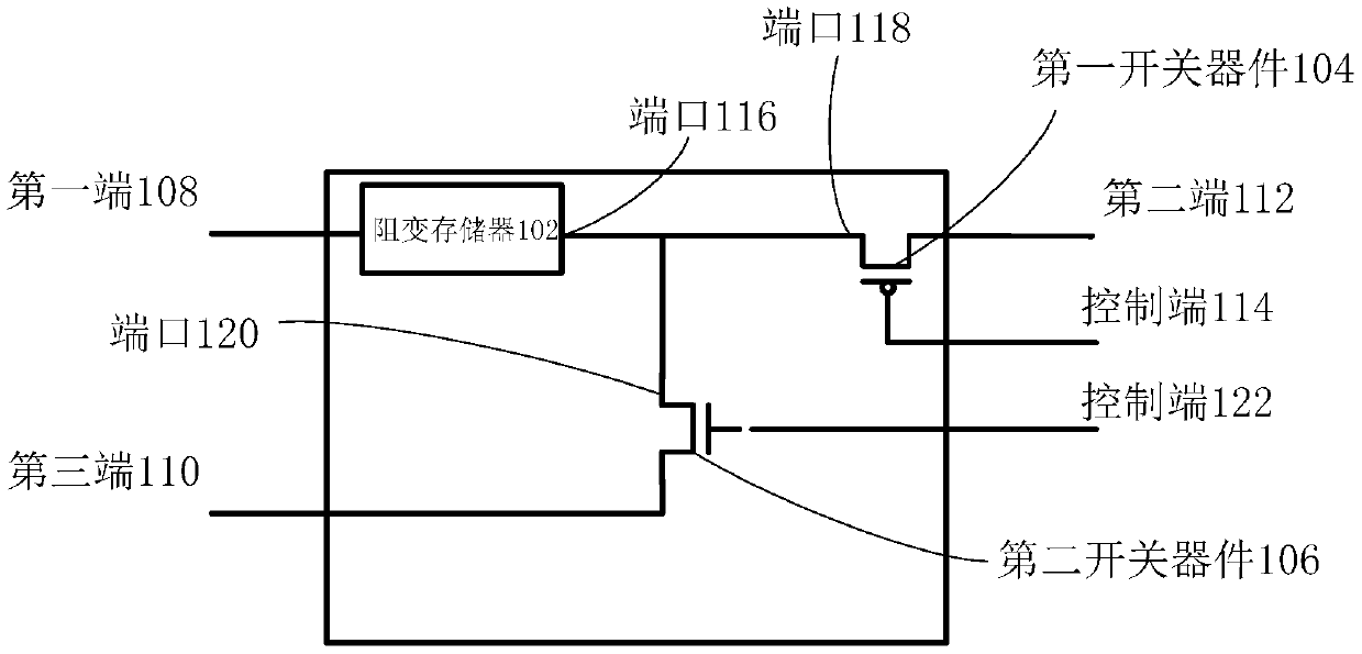
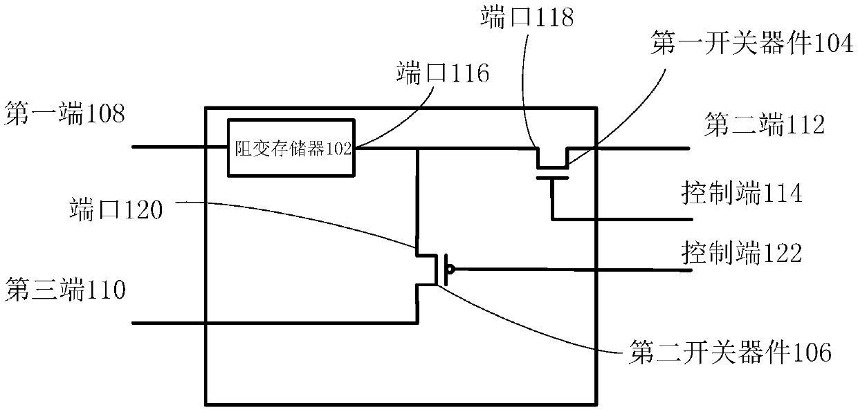
[0036] Embodiment 1 of this device provides a circuit 100 with variable resistance, the schematic diagram of its composition and structure is as follows figure 1 As shown, it includes a resistive variable memory 102 , a first switching device 104 , and a second switching device 106 .
[0037] Wherein, the two ends of the resistive variable memory 102 are respectively the first end 108 and the port 116, the first end 108 is the first end of the circuit 100, and the port 116 is respectively connected to the port 118 of the first switching device 104 and the port 116 of the second switching device 106. Port 120 is connected.
[0038] The first switching device 104 also includes a second terminal 112 and a control terminal 114, the control terminal 114 is used to receive a control signal, the control signal is used to control the first switching device on or off, that is, the second terminal 112 and the port 118 conduction or disconnection between.
[0039] The second switching ...
Embodiment 2
[0078] Embodiment 2 of this device provides a signal processing circuit 200, the schematic diagram of its composition and structure is as follows Figure 10 As shown, including the processing module 208, the circuit 202, the circuit 204, and the circuit 206, the circuit 202, the circuit 204, and the circuit 206 form a circuit group. The circuit 202 , the circuit 204 and the circuit 206 are all the circuits 100 described in any configuration mode in the first embodiment of the device. It should be noted that an actual circuit group includes at least one circuit 100 described in any of the configurations in Embodiment 1 of the device, Figure 10 The ellipsis in represents a plurality of unmarked parts as shown in the circuit 202 , meanwhile, the actual signal processing circuit 200 may include at least one circuit group, and each circuit group has the same composition.
[0079] The second ends of the circuit 202 , the circuit 204 , and the circuit 206 are connected, that is, th...
Embodiment 3
[0108] The signal processing circuit 200 described in the aforementioned second device embodiment can realize signal matching. This device embodiment is based on the second device embodiment, as Figure 12 , a more optimized signal processing circuit 300 that can be used for signal classification is proposed, and the process of using this circuit to realize signal classification is described in detail, and the specific theoretical analysis will not be described in this embodiment.
[0109] The first control terminal and the second control terminal of the circuit 100 described in any configuration of the first embodiment of each device in the signal processing circuit 300 are combined, and the circuit 100 in this case refers to the first control terminal described in the first embodiment of the device Composed way. Meanwhile, the processing module 308 also includes a port 3085 and a port 3086, which are respectively connected to the control terminal of the first circuit group and...
PUM
 Abstract
Description
Claims
Application Information
 - R&D
- Intellectual Property
- Life Sciences
- Materials
- Tech Scout
- Unparalleled Data Quality
- Higher Quality Content
- 60% Fewer Hallucinations
Browse by: Latest US Patents, China's latest patents, Technical Efficacy Thesaurus, Application Domain, Technology Topic, Popular Technical Reports.
© 2025 PatSnap. All rights reserved.Legal|Privacy policy|Modern Slavery Act Transparency Statement|Sitemap|About US| Contact US: help@patsnap.com


