Integral-imaging high-density small-interval LED display parameter design method
A technology of LED display screen and design method, applied in image communication, static indicator, identification device, etc.
- Summary
- Abstract
- Description
- Claims
- Application Information
AI Technical Summary
Problems solved by technology
Method used
Image
Examples
Embodiment Construction
[0048] The present invention will be described in detail below in conjunction with the accompanying drawings.
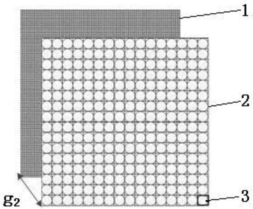
[0049] figure 1 Schematic diagram of the parameter design method for integrated imaging high-density small-pitch LED display. (1) is a high-density small-pitch LED display, (2) is a lens array, and (3) is a lens element.
[0050] figure 2 Design a schematic for the lens element template. (3) is the lens element, (4) is the base.
[0051] Suppose the shape of the lens element (3) in the lens array (2) is circular, the array is arranged, and the aperture is P 2 , the focal length is f, and the refractive index is n, then the curvature radius r and the spherical height h are respectively:
[0052] r=f(n-1) \*MERGEFORMAT(1)
[0053]
[0054] Assuming that the pixel size of the high-density small-pitch LED display screen (1) is φ, the number of pixels contained in the lens element (3) is:
[0055]
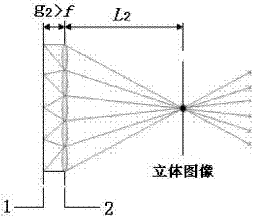
[0056] image 3 Schematic for real-mode stereoscopic displ...
PUM
 Abstract
Description
Claims
Application Information
 - R&D Engineer
- R&D Manager
- IP Professional
- Industry Leading Data Capabilities
- Powerful AI technology
- Patent DNA Extraction
Browse by: Latest US Patents, China's latest patents, Technical Efficacy Thesaurus, Application Domain, Technology Topic, Popular Technical Reports.
© 2024 PatSnap. All rights reserved.Legal|Privacy policy|Modern Slavery Act Transparency Statement|Sitemap|About US| Contact US: help@patsnap.com


