Low cost repeatable trimming method applied to integrated circuit

An integrated circuit, low-cost technology, applied in the field of low-cost repeatable trimming, can solve the problems of non-repeatable trimming, long trimming test time, and high trimming cost, saving chip area and reducing trimming test time, the effect of reducing the cost of trimming

Inactive Publication Date: 2017-09-19
聚洵半导体科技(上海)有限公司
View PDF5 Cites 1 Cited by
  • Summary
  • Abstract
  • Description
  • Claims
  • Application Information

AI Technical Summary

Problems solved by technology

[0007] Aiming at the deficiencies of the existing technology, the invention provides a low-cost repeatable trimming method applied in integrated circuits, which solves the problems of large chip area, inability to repeat trimming, long trimming test time and the The problem of high adjustment cost

Method used


Image

  • Low cost repeatable trimming method applied to integrated circuit
  • Low cost repeatable trimming method applied to integrated circuit
  • Low cost repeatable trimming method applied to integrated circuit

Examples


Embodiment Construction

[0025] The technical solutions in the embodiments of the invention will be clearly and completely described below in conjunction with the accompanying drawings in the embodiments of the invention. Obviously, the described embodiments are only part of the embodiments of the invention, not all of them. Based on the embodiments of the invention, all other embodiments obtained by persons of ordinary skill in the art without making creative efforts belong to the protection scope of the invention.

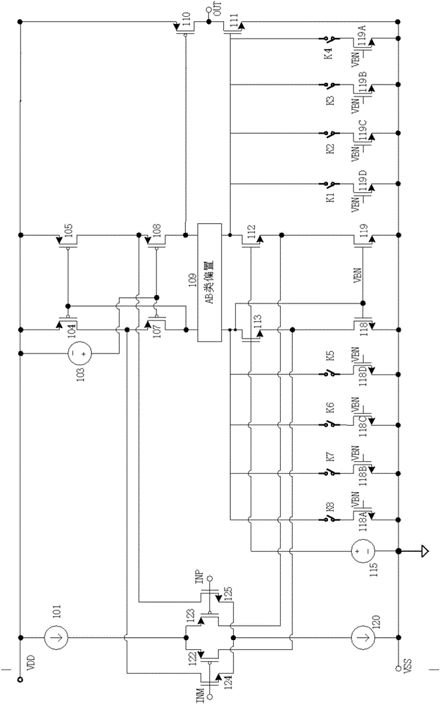
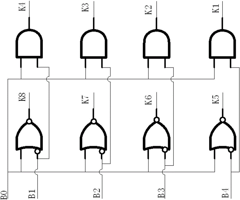
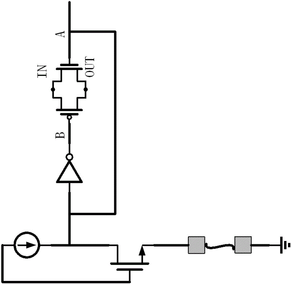
[0026] see image 3 , the invention provides a technical solution: a low-cost repeatable trimming method applied in integrated circuits, including the following process:

[0027] S1. The two input pins of the operational amplifier are multiplexed by the switch. The control signal of the switch controls the opening and closing of the switch through the trimming pad P1. On the one hand, the switch is turned off without adding a signal to the trimming pad. A pull-down signal is added to th...


PUM


Abstract

The invention discloses a low cost repeatable trimming method applied to an integrated circuit; the method comprises the following steps: S1, using a switch to reuse two input pins of an operational amplifier, and using a switch control signal to open and close the switch through trimming pads P1; S2, adding shift registers of the same number according to the trimming bit number, and reusing positive/negative input pins of the operational amplifier to provide a clock signal and a data signal of the shift register; S3, adding a control circuit of signals B0-B4. The method only needs two trimming pads to trim all bits, thus saving a chip area; the method can repeatedly repair; if errors happen in the trimming process, the trimming process can be restarted; the method only needs to trim 4 times to reach the user needed trimming precision no matter how many bits need to be trimmed, thus greatly reducing trimming testing time and trimming cost.

Description

technical field [0001] The invention relates to the technical field of circuit trimming, in particular to a low-cost repeatable trimming method applied in integrated circuits. Background technique [0002] Take operational amplifiers as an example. Operational amplifiers are widely used in consumer electronics devices, communication equipment, industrial control systems and medical devices. In many application fields, there are strict requirements on the accuracy of the input offset voltage of operational amplifiers. Some applications require operational The amplifier has a sufficiently small input offset voltage. Some applications require the operational amplifier to have a relatively fixed input offset voltage. Due to process changes and mismatch of components in integrated circuits, each chip in reality will have a different input. Therefore, it is necessary to add an input offset voltage trimming circuit in the design of the operational amplifier, and adjust the input of...

Claims


Application Information

Patent Timeline
Patent Type & Authority Applications(China)
IPC IPC(8): H03K19/003H03K19/0175
CPCH03K19/003H03K19/017509H03K19/01759
Inventor 张智才蒋宇俊
Owner 聚洵半导体科技(上海)有限公司
Why Eureka
Try Eureka