Semiconductor epitaxial wafer, method of manufacturing same, and method of manufacturing solid-state imaging device
A technology of epitaxial wafers and manufacturing methods, which is applied in semiconductor/solid-state device manufacturing, electrical components, radiation control devices, etc., can solve the problems of the limit of improvement of gettering ability, achieve superior gettering ability and suppress epitaxial defects.
- Summary
- Abstract
- Description
- Claims
- Application Information
AI Technical Summary
Problems solved by technology
Method used
Image
Examples
reference example 1
[0091] An n-type silicon wafer (diameter: 300 mm, thickness: 775 μm, doping type: phosphorus, resistivity: 20 Ω·cm) obtained from a CZ single crystal was prepared. Next, ether (C 4 h 10 O) CH after cluster ionization 3The cluster ions of O are at an accelerating voltage of 80keV / cluster (the accelerating voltage per hydrogen atom is 2.58keV / atom, the accelerating voltage per carbon atom is 30.1keV / atom, and the accelerating voltage per oxygen atom is 41.3keV / atom, The range distance (range distance) of hydrogen is 60 nm, the range distance of carbon is 120 nm, and the range distance of oxygen is 125 nm.) was irradiated on the surface of the silicon wafer under the irradiation conditions, and the silicon wafer according to Reference Example 1 was obtained. In addition, the dose of carbon when irradiating cluster ions is 1.0×10 15 Cluster / cm 2 . When converted to the number of hydrogen atoms, it is 3.0×10 15 atom / cm 2 , when converted to the number of carbon atoms, it is ...
reference example 2
[0093] In addition to irradiating cyclohexane (C 6 h 12 ) after cluster ionization of C 2 h 3 to replace the CH after ether cluster ionization in Reference Example 1 3 O and make the dose per carbon atom the same as in Reference Example 1 (i.e., the carbon dose is 1.0 × 10 15 atom / cm 2 ), cluster ion irradiation was performed under the same conditions as in Reference Example 1, and a silicon wafer according to Reference Example 2 was produced. In this case, the accelerating voltage per hydrogen atom is 2.96 keV / atom, the accelerating voltage per carbon atom is 35.6 keV / atom, the range distance of hydrogen is 60 nm, and the range distance of carbon is 120 nm.
reference example 3
[0095] Except instead of making the carbon dosage 1.0×10 in Reference Example 2 15 atom / cm 2 while making the carbon dosage 1.5×10 15 atom / cm 2 Otherwise, cluster ion irradiation was performed under the same conditions as in Reference Example 2, and a silicon wafer according to Reference Example 3 was produced.
[0096]
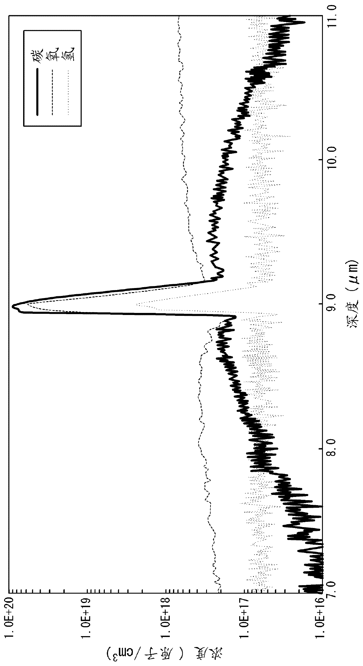
[0097] As a representative example, the silicon wafer related to Reference Example 1 was passed by quadrupole SIMS (resolution in the depth direction: 2 nm, lower limit of detection of hydrogen: 4.0×10 17 atom / cm 3 ) The concentration distribution of each of carbon, hydrogen, and oxygen in the depth direction was measured. exist image 3 The concentration distribution of Reference Example 1 is shown in . according to image 3 , the peaks of the concentration distributions of hydrogen, carbon, and oxygen were observed in the depth direction from the surface side of the silicon wafer.
[0098]
[0099] For each of the silicon wafers in Reference Exa...
PUM
| Property | Measurement | Unit |
|---|---|---|
| thickness | aaaaa | aaaaa |
| depth | aaaaa | aaaaa |
| size | aaaaa | aaaaa |
Abstract
Description
Claims
Application Information
 - R&D
- Intellectual Property
- Life Sciences
- Materials
- Tech Scout
- Unparalleled Data Quality
- Higher Quality Content
- 60% Fewer Hallucinations
Browse by: Latest US Patents, China's latest patents, Technical Efficacy Thesaurus, Application Domain, Technology Topic, Popular Technical Reports.
© 2025 PatSnap. All rights reserved.Legal|Privacy policy|Modern Slavery Act Transparency Statement|Sitemap|About US| Contact US: help@patsnap.com


